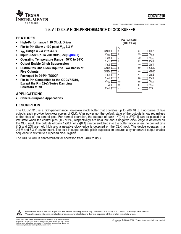
CDCVF310 Overview
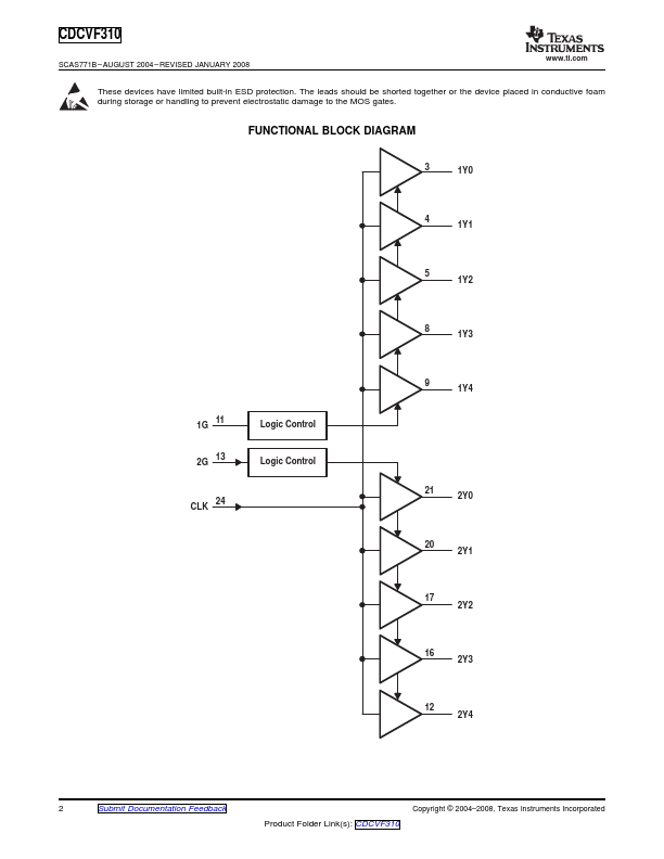
The CDCVF310 is a high-performance, low-skew clock buffer that operates up to 200 MHz. Two banks of five outputs each provide low-skew copies of CLK. After power up, the default state of the outputs is low regardless of the state of the control pins.
CDCVF310 Key Features
- High-Performance 1:10 Clock Driver
- Pin-to-Pin Skew < 100 ps at VDD 3.3 V
- VDD Range = 2.3 V to 3.6 V
- Input Clock Up To 200 MHz (See Figure 7)
- Operating Temperature Range -40°C to 85°C
- Output Enable Glitch Suppression
- Packaged in 24-Pin TSSOP
- Pin-to-Pin patible to the CDCVF2310