CSD17575Q3 Overview
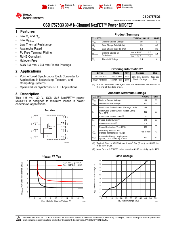
This 1.9 mΩ, 30 V, SON 3×3 NexFET™ power MOSFET is designed to minimize losses in power conversion applications. CSD17575Q3 SLPS489A JUNE 2014 REVISED AUGUST 2014 .ti.
CSD17575Q3 Key Features
- 1 Low Qg and Qgd
- Low RDS(on)
- Low Thermal Resistance
- Avalanche Rated
- Pb Free Terminal Plating
- RoHS pliant
- Halogen Free
- SON 3.3 mm × 3.3 mm Plastic Package
CSD17575Q3 Applications
- Point of Load Synchronous Buck Converter for Applications in Networking, Tele, and puting Systems
- Optimized for Synchronous FET Applications