CSD18511Q5A
CSD18511Q5A is power MOSFET manufactured by Texas Instruments.
Features
- 1 Low RDS(ON)
- Low Thermal Resistance
- Avalanche Rated
- Logic Level
- Pb Free Terminal Plating
- Ro HS pliant
- Halogen Free
- SON 5-mm × 6-mm Plastic Package
2 Applications
- DC-DC Conversion
- Secondary Side Synchronous Rectifier
- Battery Motor Control
Product Summary
TA = 25°C VDS Drain-to-Source Voltage Qg Gate Charge Total (10 V) Qgd Gate Charge Gate-to-Drain
RDS(on) Drain-to-Source On-Resistance
VGS(th) Threshold Voltage
TYPICAL VALUE
VGS = 4.5 V VGS = 10 V
2.7 1.9
UNIT V n C n C mΩ mΩ V
Ordering Information(1)
Device
Qty Media
Package
CSD18511Q5A 2500 13-Inch Reel SON 5 mm × 6 mm
CSD18511Q5AT 250 7-Inch Reel
Plastic Package
Ship
Tape and Reel
(1) For all available packages, see the orderable addendum at the end of the data sheet.
3 Description
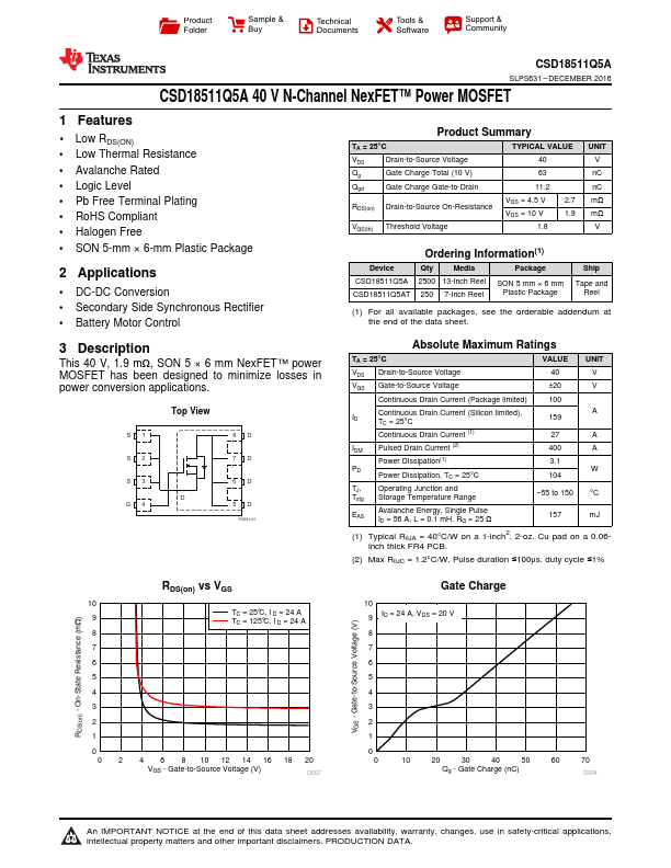
This 40 V, 1.9 mΩ, SON 5 × 6 mm Nex FET™ power MOSFET has been designed to minimize losses in power conversion applications.
Top...