SN65DSI84-Q1
Overview
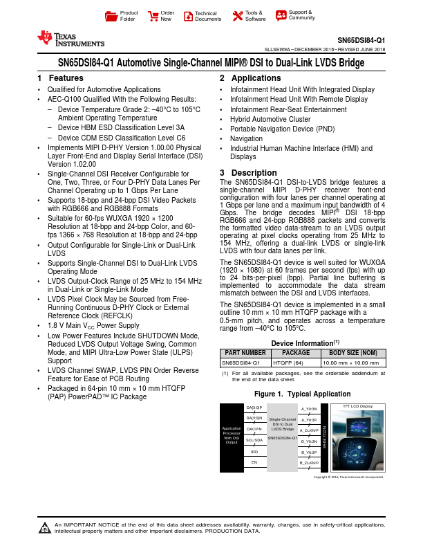
The SN65DSI84-Q1 DSI-to-LVDS bridge features a single-channel MIPI D-PHY receiver f.
- 1 Qualified for Automotive Applications
- AEC-Q100 Qualified With the Following Results: - Device Temperature Grade 2: -40°C to 105°C Ambient Operating Temperature - Device HBM ESD Classification Level 3A - Device CDM ESD Classification Level C6
- Implements MIPI D-PHY Version 1.00.00 Physical Layer Front-End and Display Serial Interface (DSI) Version 1.02.00
- Single-Channel DSI Receiver Configurable for One, Two, Three, or Four D-PHY Data Lanes Per Channel Operating up to 1 Gbps Per Lane
- Supports 18-bpp and 24-bpp DSI Video Packets with RGB666 and RGB888 Formats
- Suitable for 60-fps WUXGA 1920 × 1200 Resolution at 18-bpp and 24-bpp Color, and 60fps 1366 × 768 Resolution at 18-bpp and 24-bpp
- Output Configurable for Single-Link or Dual-Link LVDS
- Supports Single-Channel DSI to Dual-Link LVDS Operating Mode
- LVDS Output-Clock Range of 25 MHz to 154 MHz in Dual-Link or Single-Link Mode
- LVDS Pixel Clock May be Sourced from FreeRunning Continuous D-PHY Clock or External Reference Clock (REFCLK)