Datasheet4U Logo Datasheet4U.com

SN74LVC1G11 - Single 3-Input Positive-AND Gate

General Description

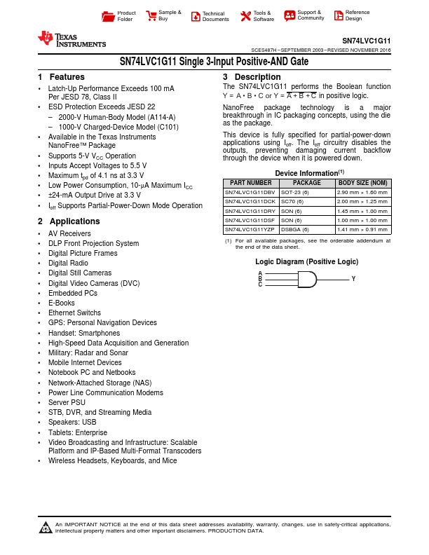
The SN74LVC1G11 performs the Boolean function Y = A B

C or Y = A + B + C in positive logic.

NanoFree package technology is a major breakthrough in IC packaging concepts, using the die as the package.

This device is fully specified for partial-power-down applications using Ioff.

Key Features

  • 1 Latch-Up Performance Exceeds 100 mA Per JESD 78, Class II.
  • ESD Protection Exceeds JESD 22.
  • 2000-V Human-Body Model (A114-A).
  • 1000-V Charged-Device Model (C101).
  • Available in the Texas Instruments NanoFree™ Package.
  • Supports 5-V VCC Operation.
  • Inputs Accept Voltages to 5.5 V.
  • Maximum tpd of 4.1 ns at 3.3 V.
  • Low Power Consumption, 10-μA Maximum ICC.
  • ±24-mA Output Drive at 3.3 V.
  • Ioff Supports Parti.

📥 Download Datasheet

Full PDF Text Transcription (Reference)

The following content is an automatically extracted verbatim text from the original manufacturer datasheet and is provided for reference purposes only.

View original datasheet text
Product Folder Sample & Buy Technical Documents Tools & Software Support & Community Reference Design SN74LVC1G11 SCES487H – SEPTEMBER 2003 – REVISED NOVEMBER 2016 SN74LVC1G11 Single 3-Input Positive-AND Gate 1 Features •1 Latch-Up Performance Exceeds 100 mA Per JESD 78, Class II • ESD Protection Exceeds JESD 22 – 2000-V Human-Body Model (A114-A) – 1000-V Charged-Device Model (C101) • Available in the Texas Instruments NanoFree™ Package • Supports 5-V VCC Operation • Inputs Accept Voltages to 5.5 V • Maximum tpd of 4.1 ns at 3.3 V • Low Power Consumption, 10-μA Maximum ICC • ±24-mA Output Drive at 3.