• Part: TPIC6C595
  • Description: Power Logic 8-Bit Shift Register
  • Manufacturer: Texas Instruments
  • Size: 1.28 MB
Download TPIC6C595 Datasheet PDF
Texas Instruments
TPIC6C595
TPIC6C595 is Power Logic 8-Bit Shift Register manufactured by Texas Instruments.
Features - 1 Low r DS(on), 7 Ω Typical - Avalanche Energy, 30 m J - Eight Power DMOS Transistor Outputs of 100-m A Continuous Current - 250-m A Current Limit Capability - ESD Protection, 2500 V - Output Clamp Voltage, 33 V - Devices are Cascadable - Low-Power Consumption Outputs are low-side, open-drain DMOS transistors with output ratings of 33-V to 100-m A continuous sink-current capability. Each output provides a 250-m A maximum current limit at TC = 25°C. The current limit decreases as the junction temperature increases for additional device protection. The device also provides up to 2500 V of ESD protection when tested using the human-body model and the 200-V machine model. The TPIC6C595 is characterized for operation over the operating case temperature range of - 40°C to 125°C. 2 Applications - Instrumentation Clusters - Tell-Tale Lamps - LED Illumination and Controls - Automotive Relay or Solenoids - Drivers PART NUMBER TPIC6C595 Device Information(1) PACKAGE BODY SIZE (NOM) SOIC (16) 9.90 mm × 3.91 mm TSSOP (16) 5.00 mm × 4.40 mm PDIP (16) 19.30 mm × 6.35 mm (1) For all available packages, see the orderable addendum at the end of the data sheet. 3 Description 
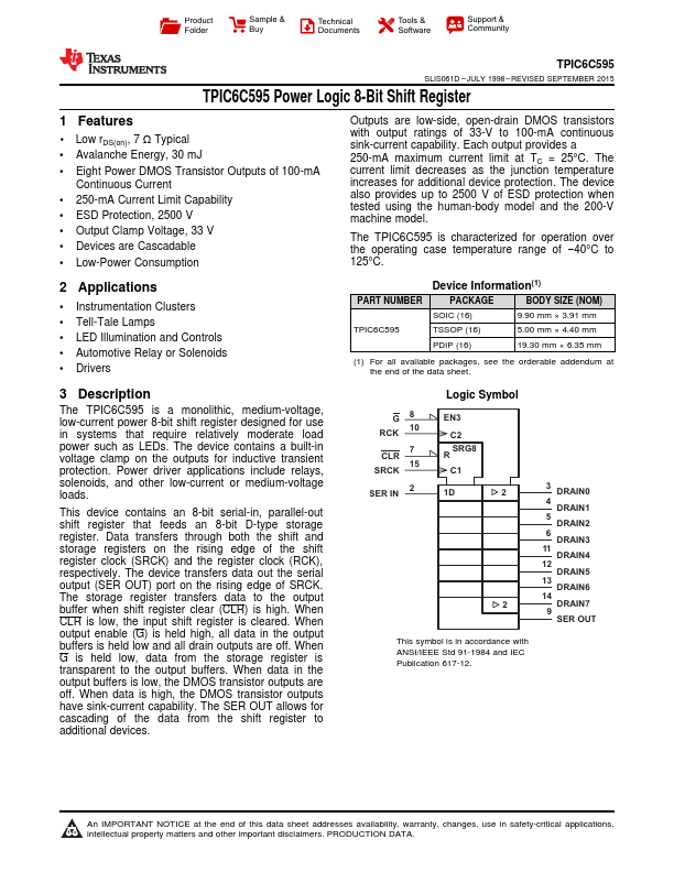
The TPIC6C595 is a monolithic, medium-voltage, low-current power 8-bit shift register designed for use in systems that require relatively moderate load power such as LEDs. The device contains a built-in voltage clamp on the outputs for inductive transient protection. Power driver applications include relays, solenoids, and other low-current or medium-voltage loads. This device contains an 8-bit serial-in, parallel-out shift register that feeds an 8-bit D-type storage register. Data transfers through both the shift and storage registers on the rising edge of the shift register clock (SRCK) and the register clock (RCK), respectively. The device transfers data out the serial output (SER OUT) port on the rising edge of SRCK. The storage register transfers data to the output buffer when shift register...