onsemi 2N6609
COMPLEMENTARY POWER TRANSISTORS
| Part No. | 2N6609 |
|---|---|
| Datasheet | 2N6609 Download |
| Manufacturer |  onsemi |
| Description | COMPLEMENTARY POWER TRANSISTORS |
| Buy | Stock & Price |

FEATURES
●●
●
●
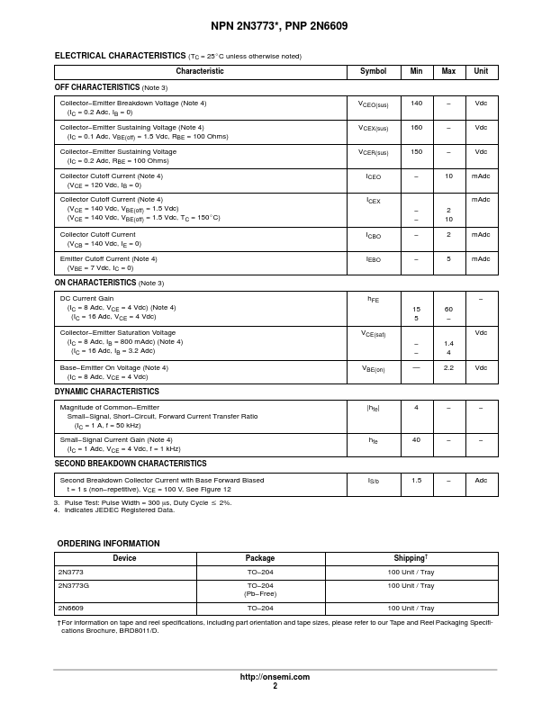
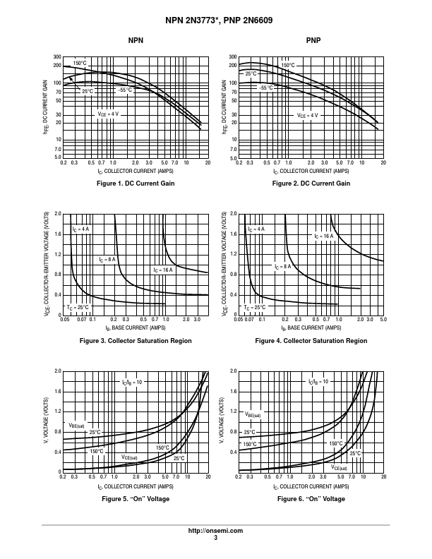
● Pb−Free Packages are Available** High Safe Operating Area (100% Tested) 150 W @ 100 V Completely Characterized for Linear Operation High DC Current Gain and Low Saturation Voltage hFE = 15 (Min) @ 8.0 A, 4.0 V VCE(sat) = 1.4 V (Max) @ IC = 8.0 A, IB = 0.8 A For Low Distortion Complementary Designs 16 A COMPLEMENTARY POWER TRANSISTORS 140 V, 150 W MARKING DIAGRAM
MAXIMUM RATINGS
(Note 1) Rating Collector − Emitter Voltage Collector − Emitter Voltage Collector − Base Voltage Emitter − Base Voltage Collector Current − Continuous − Peak (Note 2) Base Current − Continuous − Peak (Note 2) Total Power Dissipation @ TA = 25°C Derate above 25°C Operating and Storage Junction Temperature Range PD TJ, Tstg Symbol VCEO VCEX VCBO VEBO IC 16 30 IB 4 15 150 0.855 −65 to +200 W W/°C °C Adc Value 140 160 160 7 Unit Vdc Vdc Vdc Vdc Adc xxxx A YY WW TO−204 CASE 1−07 2Nxxxx MEX AYYWW = 3773 or 6609 = Assembly Location = Year = Work Week ORDERING INFORMATION See detailed ordering and shi...