onsemi 2N7002W
Small Signal MOSFET
| Part No. | 2N7002W |
|---|---|
| Datasheet | 2N7002W Download |
| Manufacturer |  onsemi |
| Description | Small Signal MOSFET |
| Buy | Stock & Price |
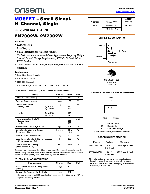
FEATURES
● ESD Protected● Low RDS(on)
● Small Footprint Surface Mount Package
● 2V Prefix for Automotive and Other
APPLICATIONS
Requiring Unique Site and Control Change Requirements; AEC−Q101 Qualified and PPAP Capable● These Devices are Pb−Free, Halogen Free/BFR Free and are RoHS Compliant
APPLICATIONS
● Low Side Load Switch● Level Shift Circuits
● DC−DC Converter
● Portable
APPLICATIONS
i.e. DSC, PDA, Cell Phone, etc.MAXIMUM RATINGS
(TJ = 25C unless otherwise stated) Rating Symbol Value Unit Drain−to−Source Voltage Gate−to−Source Voltage Drain Current (Note 1) Steady State VDSS 60 V VGS 20 V ID TA = 25C TA = 85C mA 310 220 t<5s Power Dissipation (Note 1) Steady State t<5s TA = 25C TA = 85C PD 340 240 mW 280 330 Pulsed Drain Current (tp = 10 ms) Operating Junction and Storage Temperature Range IDM 1.4 A TJ, TSTG −55 to C +150 Source Current (Body Diode) IS 250 mA Lead Temperature for Soldering Purposes TL 260 C (1/8● from case for 10 s) Gate−Source ESD Rating (HBM, Method 3015) ESD 2000 V Stresses exceeding those listed in theMAXIMUM RATINGS
table may damage the device.