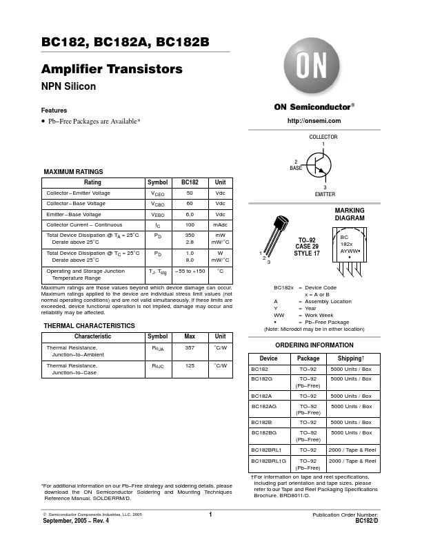
BC182A
Overview
- Pb-Free Packages are Available*
| Part | BC182A |
|---|---|
| Description | NPN Silicon Amplifier Transistors |
| Category | Transistor |
| Manufacturer | onsemi |
| Size | 50.39 KB |
| Part Number | Manufacturer | Description |
|---|---|---|
| BC182A | Motorola Semiconductor | Amplifier Transistors |
| BC182A | Continental Device India | NPN SILICON PLANAR EPITAXIAL TRANSISTORS |
| BC182 | Central Semiconductor | SILICON NPN TRANSISTOR |
| BC182B | Continental Device India | NPN SILICON PLANAR EPITAXIAL TRANSISTORS |
| BC182 | Fairchild Semiconductor | AMPLIFIER TRANSISTOR |