onsemi IRF530
Power Field Effect Transistor
| Part No. | IRF530 |
|---|---|
| Datasheet | IRF530 Download |
| Manufacturer |  onsemi |
| Description | Power Field Effect Transistor |
| Buy | Stock & Price |
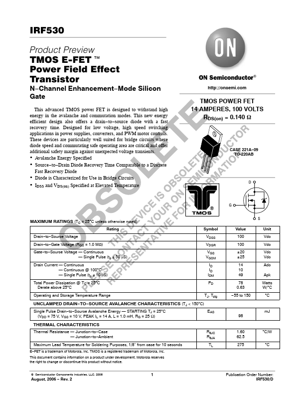
MAXIMUM RATINGS
(TC = 25°C unless otherwise noted) Rating Symbol Drain−to−Source Voltage Drain−to−Gate Voltage (RGS = 1.0 MΩ) Gate−to−Source Voltage — Continuous Gate−to−Source Voltage — Single Pulse (tp ≤ 50 mS) Drain Current — Continuous Drain Current — Continuous @ 100°C Drain Current — Single Pulse (tp ≤ 10 mS) Total Power Dissipation @ TC = 25°C Derate above 25°C VDSS VDGR VGS VGSM ID ID IDM PD Operating and Storage Temperature Range TJ, Tstg UNCLAMPED DRAIN−TO−SOURCE AVALANCHE CHARACTERISTICS (TJ < 150°C) Single Pulse Drain−to−Source Avalanche Energy — STARTING TJ = 25°C (VDD = 75 V, VGS = 10 V, PEAK IL = 14 A, L = 1.0 mH, RG = 25 W) EAS THERMAL CHARACTERISTICS Thermal Resistance — Junction−to−Case° Thermal Resistance — Junction−to−Ambient° Maximum Lead Temperature for Soldering Purposes, 1/8″ from case for 10 seconds E−FET is a trademark of Motorola, Inc. TMOS is a registered trademark of Motorola, Inc. This document contains information on a product under development. Motorola reserves the right to change or discontinue this product without notice.