PED3018MAT
PED3018MAT is N-Channel Enhancement Mode Power MOSFET manufactured by semi one.
Description
The PED3018MAT uses advanced trench technology to provide excellent RDS(ON) and low gate charge. It can be used in a wide variety of applications.
General Features
- VDS = 30V, ID = 80A
RDS(ON) < 3.8mΩ @ VGS=10V RDS(ON) < 6.5mΩ @ VGS=4.5V
- High Power and current handing capability
- Lead free product is acquired
- Surface Mount Package
Application
- Battery management
- Motor controller and driver
- PWM applications
- Load switch
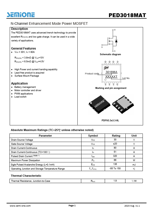
Schematic diagram Marking and pin assignment
PDFN3.3x3.3-8L
Absolute Maximum Ratings (TC=25℃ unless otherwise noted)
Parameter
Drain-Source Voltage Gate-Source Voltage Drain Current-Continuous Drain Current-Continuous (TC=100℃) Pulsed Drain Current (Note 1) Maximum Power Dissipation Sigle Pulsed Avalanche Energy (L=0.1m H) Operating Junction and Storage Temperature Range
Symbol
VDS VGS ID ID IDM PD EAS TJ,TSTG
Thermal Characteristic
Thermal Resistance, Junction-to-Case
RθJC
Rating
30 ±20 80 51 320 66 135 -55 To 150
Unit
V V A A A W m J ℃
℃/W
.semi-one.
Page 1
2023 Aug. v1.1
Electrical Characteristics (TC=25℃ unless otherwise noted)
Parameter
Off Characteristics Drain-Source Breakdown Voltage Zero Gate Voltage Drain Current Gate-Body Leakage Current On Characteristics (Note 3) Gate Threshold Voltage
Drain-Source On-State Resistance
Forward Transconductance Dynamic Characteristics (Note 4) Input Capacitance Output Capacitance Reverse Transfer Capacitance (Note 4) Gate Resistance Switching Characteristics Turn-on Delay Time Turn-on Rise Time Turn-Off Delay Time Turn-Off Fall Time Total Gate Charge Gate-Source Charge Gate-Drain Charge Drain-Source Diode Characteristics Diode Forward Voltage (Note 3) Diode Forward Current (Note 2) Body Diode Reverse Recovery Time Body Diode Reverse Recovery Charge
Symbol
Condition
Min Typ Max...