CD4050BM Datasheet
CD4050BM Datasheet (National Semiconductor)
National Semiconductor
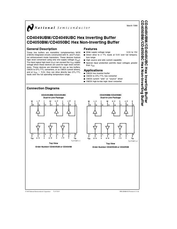
These hex buffers are monolithic complementary MOS (CMOS) integrated circuits constructed with N- and P-channel enhancement mode transistors These devices feature logic level conversion using only one.
Y Y Y Y Wide supply voltage range 3 0V to 15V Direct drive to 2 TTL loads at 5 0V over full temperature range High source and sink current capability Special input protection permits input voltages greater than VDD Applications Y Y Y Y CMOS CMOS CMOS CMOS hex inverter buffer to DTL TTL hex conv.
CD4050BM Datasheet (Texas Instruments)
Texas Instruments
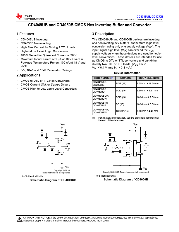
The CD4049UB and CD4050B devices are inverting and noninverting hex buffers, and feature logic-level conversion using only one supply voltage (VCC). The input-signal high level (VIH) can exceed the V.
* CD4049UB Inverting
* CD4050B Noninverting
* High Sink Current for Driving 2 TTL Loads
* High-to-Low Level Logic Conversion
* 100% Tested for Quiescent Current at 20 V
* Maximum Input Current of 1 µA at 18 V Over Full
Package Temperature Range; 100 nA at 18 V and 25°C
* 5-V, 10-V, and 15-V Parametr.