Datasheet4U Logo Datasheet4U.com

AS4C32M32MD2A-25BIN - 1G (64M x 16 and 32M x 32) Low Power DDR2 SDRAM

Key Features

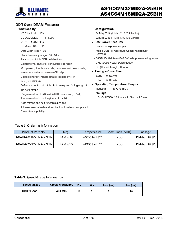
  • Functionality - VDD2 = 1.14.
  • 1.30V - VDDCA/VDDQ = 1.14.
  • 1.30V - VDD1 = 1.70.
  • 1.95V - Interface : HSUL_12 - Data width : x16 / x32 - Clock frequency range : 400 MHz - Four-bit pre-fetch DDR architecture - Eight internal banks for concurrent operation - Multiplexed, double data rate, command/address inputs; commands entered on every CK edge - Bidirectional/differential data strobe per byte of data(DQS/DQS#). - DM masks write date at the both rising and fallin.

📥 Download Datasheet

Datasheet Details

Part number AS4C32M32MD2A-25BIN
Manufacturer Alliance Semiconductor
File Size 5.49 MB
Description 1G (64M x 16 and 32M x 32) Low Power DDR2 SDRAM
Datasheet download datasheet AS4C32M32MD2A-25BIN Datasheet

Full PDF Text Transcription (Reference)

The following content is an automatically extracted verbatim text from the original manufacturer datasheet and is provided for reference purposes only.

View original datasheet text
AS4C32M32MD2A-25BIN AS4C64M16MD2A-25BIN Revision History 1G (64M x 16 and 32M x 32) Low Power DDR2 SDRAM 134ball FBGA Package AS4C64M16MD2A-25BIN/AS4C32M32MD2A-25BIN Revision Details Rev 1.0 Preliminary datasheet Date Jan 2018 Alliance Memory Inc. 511 Taylor Way, San Carlos, CA 94070 TEL: (650) 610-6800 FAX: (650) 620-9211 Alliance Memory Inc. reserves the right to change products or specification without notice Confidential - 1 of 125 - Rev.1.0 Jan. 2018 AS4C32M32MD2A-25BIN AS4C64M16MD2A-25BIN DDR Sync DRAM Features • Functionality - VDD2 = 1.14–1.30V - VDDCA/VDDQ = 1.14–1.30V - VDD1 = 1.70–1.