AS4C64M16MD2A-25BIN Description
511 Taylor Way, San Carlos, CA 94070 TEL: (650) 620-9211 Alliance Memory Inc. reserves the right to change products or specification without notice Confidential - 1 of 125 - Rev.1.0 Jan.
AS4C64M16MD2A-25BIN Key Features
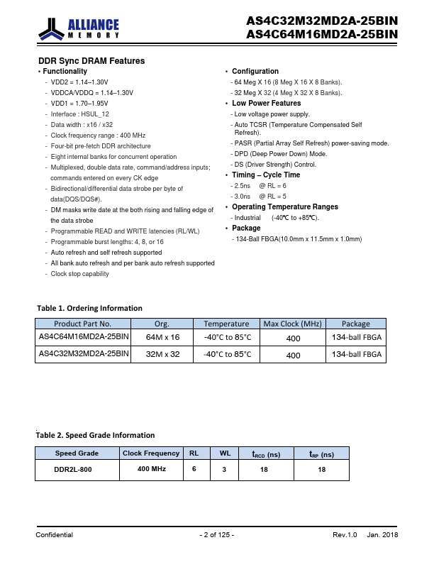
- Functionality
- VDD2 = 1.14-1.30V
- VDDCA/VDDQ = 1.14-1.30V
- VDD1 = 1.70-1.95V
- Interface : HSUL_12
- Data width : x16 / x32
- Clock frequency range : 400 MHz
- Four-bit pre-fetch DDR architecture
- Eight internal banks for concurrent operation
- Multiplexed, double data rate, mand/address inputs; mands entered on every CK edge