AS7C33512PFS36A Key Features
- Individual byte write and global write Multiple chip enables for easy expansion 3.3V core power supply 2.5V or 3.3V I/O
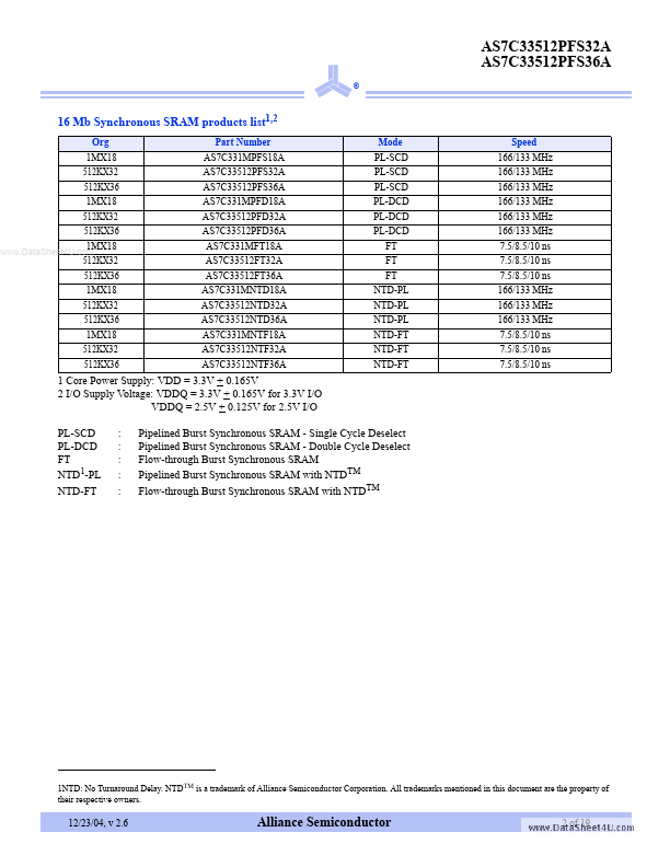
- Single Cycle Deselect Pipelined Burst Synchronous SRAM
- Double Cycle Deselect Flow-through Burst Synchronous SRAM Pipelined Burst Synchronous SRAM with NTDTM Flow-through Burst
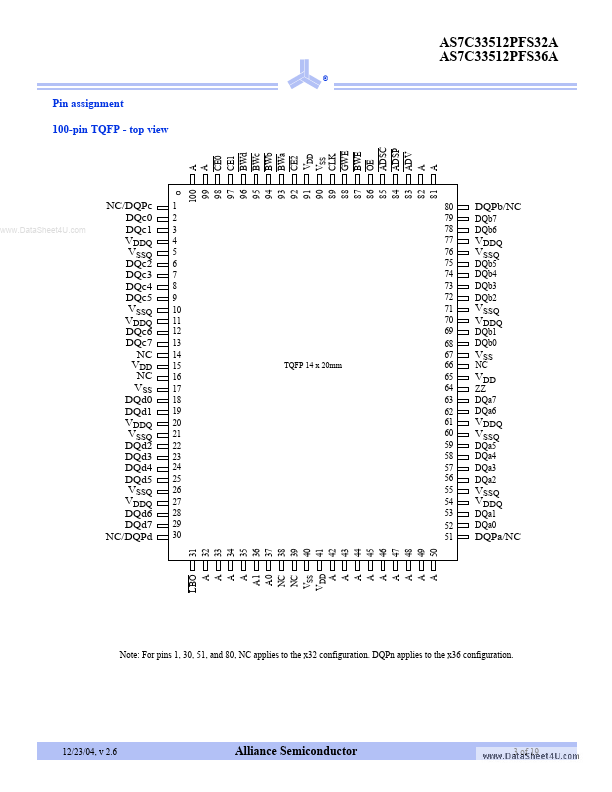
- top view