AO4422
Description
The AO4422 uses advanced trench technology to provide excellent RDS(ON) and low gate charge. This device is suitable for use as a load switch or in PWM applications. The source leads are separated to allow a Kelvin connection to the source, which may be used to bypass the source inductance.
Features
VDS (V) = 30V ID = 11A RDS(ON) < 15mΩ (VGS = 10V) RDS(ON) < 24mΩ (VGS = 4.5V)
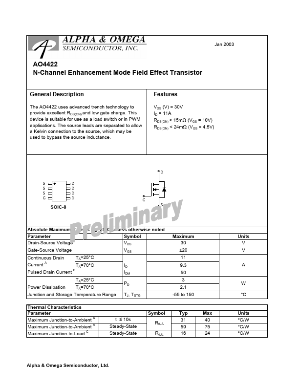
SD SD SD GD
SOIC-8
Absolute Maximum Ratings TA=25°C unless otherwise noted
Parameter
Symbol
Drain-Source Voltage
Gate-Source Voltage
Continuous Drain
TA=25°C
Current A
TA=70°C
Pulsed Drain Current B
ID IDM
Power Dissipation
TA=25°C TA=70°C
Junction and Storage Temperature Range TJ, TSTG
Maximum 30 ±20 11 9.3 50 3 2.1
-55 to 150
Thermal Characteristics Parameter Maximum Junction-to-Ambient A Maximum Junction-to-Ambient A
Maximum Junction-to-Lead C t ≤ 10s Steady-State...