Datasheet Details
| Part number | AO4447A |
|---|---|
| Manufacturer | Alpha & Omega Semiconductors |
| File Size | 258.67 KB |
| Description | 30V P-Channel MOSFET |
| Download | AO4447A Download (PDF) |
|
|
| Part number | AO4447A |
|---|---|
| Manufacturer | Alpha & Omega Semiconductors |
| File Size | 258.67 KB |
| Description | 30V P-Channel MOSFET |
| Download | AO4447A Download (PDF) |
|
|
|
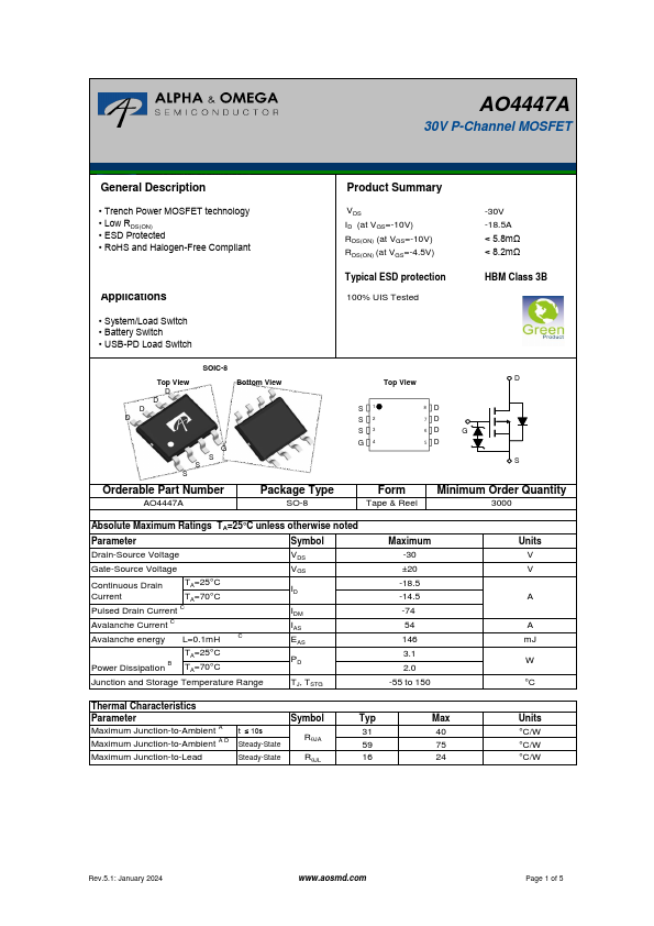
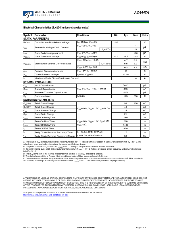
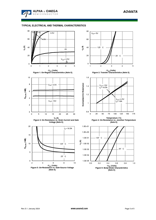
• Trench Power MOSFET technology • Low RDS(ON) • ESD Protected • RoHS and Halogen-Free Compliant Applications Product Summary VDS ID (at VGS=-10V) RDS(ON) (at VGS=-10V) RDS(ON) (at VGS=-4.5V) Typical ESD protection 100% UIS Tested -30V -18.5A < 5.8mΩ < 8.2mΩ HBM Class 3B • System/Load Switch • Battery Switch • USB-PD Load Switch Top View D D D D SOIC-8 Bottom View G S S S Orderable Part Number AO4447A Package Type SO-8 Top View D S1 S2 S3 G4 8D 7D 6D G 5D S Form Minimum Order Quantity Tape & Reel 3000 Absolute Maximum Ratings TA=25°C unless otherwise noted Parameter Symbol Drain-Source Voltage VDS Gate-Source Voltage VGS Continuous Drain Current TA=25°C TA=70°C ID Pulsed Drain Current C IDM Avalanche Current C IAS Avalanche energy L=0.1mH C EAS TA=25°C Power Dissipation B TA=70°C PD Junction and Storage Temperature Range TJ, TSTG Maximum -30 ±20 -18.5 -14.5 -74 54 146 3.1 2.0 -55 to 150 Units V V A A mJ W °C Thermal Characteristics Parameter Symbol Typ Maximum Junction-to-Ambient A t ≤ 10s Maximum Junction-to-Ambient A D Steady-State RqJA 31 59 Maximum Junction-to-Lead Steady-State RqJL 16 Max 40 75 24 Units °C/W °C/W °C/W Rev.5.1: January 2024 www.aosmd.com Page 1 of 5 AO4447A Electrical Characteristics (TJ=25°C unless otherwise noted) Symbol Parameter Conditions Min STATIC PARAMETERS BVDSS Drain-Source Breakdown Voltage ID=-250mA, VGS=0V -30 IDSS Zero Gate Voltage Drain Current VDS=-30V, VGS=0V TJ=55°C IGSS Gate-Body leakage current VDS=0V, VGS=±16V VGS(th) Gate Threshold Voltage VDS=VGS, ID=-250mA -1.2 VGS=-10V, ID=-18.5A RDS(ON) Static Drain-Source On-Resistance TJ=125°C VGS=-4.5V, ID=-16A gFS Forward Transconductance VDS=-5V, ID=-18.5A VSD Diode Forward Voltage IS=-1A, VGS=0V IS Maximum Body-Diode Continuous Current DYNAMIC PARAMETERS Ciss Input Capacitance Coss Output Capacitance Crss Reverse Transfer Capacitance Rg
AO4447A 30V P-Channel MOSFET General.
| Brand Logo | Part Number | Description | Manufacturer |
|---|---|---|---|
| AO4447A | P-Channel MOSFET | Kexin | |
| AO4447A-HF | P-Channel MOSFET | Kexin | |
| AO4447 | P-Channel 30V MOSFET | VBsemi | |
| AO4447 | P-Channel MOSFET | Kexin |
| Part Number | Description |
|---|---|
| AO4447 | P-Channel MOSFET |
| AO4440 | N-Channel MOSFET |
| AO4441 | 60V P-Channel MOSFET |
| AO4442 | N-Channel MOSFET |
| AO4443 | 40V P-Channel MOSFET |
| AO4444 | N-Channel MOSFET |
| AO4444L | 80V N-Channel MOSFET |
| AO4446 | N-Channel MOSFET |
| AO4448 | 80V N-Channel MOSFET |
| AO4448L | 80V N-Channel MOSFET |