Datasheet Details
| Part number | AOD4184 |
|---|---|
| Manufacturer | Alpha & Omega Semiconductors |
| File Size | 400.38 KB |
| Description | 40V N-Channel MOSFET |
| Download | AOD4184 Download (PDF) |
|
|
| Part number | AOD4184 |
|---|---|
| Manufacturer | Alpha & Omega Semiconductors |
| File Size | 400.38 KB |
| Description | 40V N-Channel MOSFET |
| Download | AOD4184 Download (PDF) |
|
|
|
Product Summary The AOD4184/AOI4184 used advanced trench technology and design to provide excellent RDS(ON) with low gate charge.
With the excellent thermal resistance of the DPAK package, those devices are well suited for high current load applications.
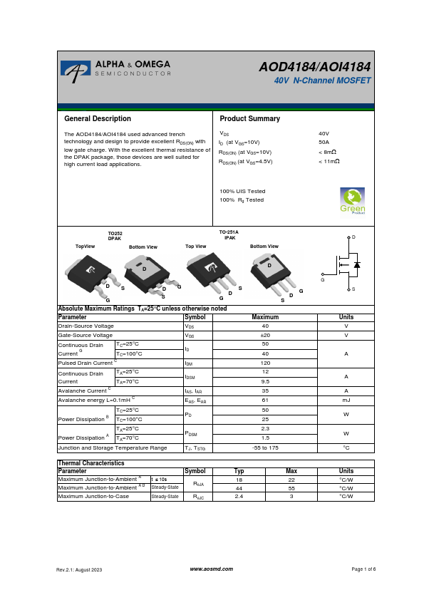
VDS ID (at VGS=10V) RDS(ON) (at VGS=10V) RDS(ON) (at VGS=4.5V) 100% UIS Tested 100% Rg Tested 40V 50A < 8mW < 11mW TopView TO252 DPAK Bottom View Top View TO-251A IPAK Bottom View D D DS G DG S S D G Absolute Maximum Ratings TA=25°C unless otherwise noted Parameter Symbol Drain-Source Voltage VDS Gate-Source Voltage Continuous Drain TC=25°C Current G TC=100°C Pulsed Drain Current C Continuous Drain Current Avalanche Current C TA=25°C TA=70°C Avalanche energy L=0.1mH C VGS ID IDM IDSM IAS, IAR EAS, EAR TC=25°C Power Dissipation B TC=100°C PD TA=25°C Power Dissipation A TA=70°C PDSM Junction and Storage Temperature Range TJ, TSTG G D S Maximum 40 ±20 50 40 120 12 9.5 35 61 50 25 2.3 1.5 -55 to 175 Thermal Characteristics Parameter Symbol Typ Maximum Junction-to-Ambient A t ≤ 10s Maximum Junction-to-Ambient A D Steady-State RqJA 18 44 Maximum Junction-to-Case Steady-State RqJC 2.4 Max 22 55 3 D G S Units V V A A A mJ W W °C Units °C/W °C/W °C/W Rev.2.1: August 2023 www.aosmd.com Page 1 of 6 AOD4184/AOI4184 Electrical Characteristics (TJ=25°C unless otherwise noted) Symbol Parameter Conditions Min Typ Max Units STATIC PARAMETERS BVDSS Drain-Source Breakdown Voltage ID=250mA, VGS=0V 40 V IDSS Zero Gate Voltage Drain Current VDS=40V, VGS=0V TJ=55°C 1 5 mA IGSS Gate-Body leakage current VDS=0V, VGS=±20V ±100 nA VGS(th) Gate Threshold Voltage VDS=VGS ID=250mA 1.7 2.2 2.6 V ID(ON) On state drain current VGS=10V, VDS=5V 120 A RDS(ON) Static Drain-Source On-Resistance VGS=10V, ID=20A TJ=125°C 6.7 8 11 13 mW VGS=4.5V, ID=15A 8.5 11 mW gFS Forward Transconductance VDS=5V, ID=20
AOD4184/AOI4184 40V N-Channel MOSFET General.
| Brand Logo | Part Number | Description | Manufacturer |
|---|---|---|---|
| AOD4184 | N-Channel MOSFET | INCHANGE | |
| AOD4184 | N-Channel MOSFET | VBsemi | |
| AOD4184A | N-Channel MOSFET | INCHANGE |
| Part Number | Description |
|---|---|
| AOD4184A | 40V N-Channel MOSFET |
| AOD418 | 30V N-Channel MOSFET |
| AOD4180 | 80V N-Channel MOSFET |
| AOD4182 | 80V N-Channel MOSFET |
| AOD4185 | 40V P-Channel MOSFET |
| AOD4186 | 40V N-Channel MOSFET |
| AOD4187 | P-Channel MOSFET |
| AOD4189 | P-Channel MOSFET |
| AOD410 | N-Channel MOSFET |
| AOD4100 | N-Channel MOSFET |