Datasheet Details
| Part number | AON2410 |
|---|---|
| Manufacturer | Alpha & Omega Semiconductors |
| File Size | 247.72 KB |
| Description | 30V N-Channel MOSFET |
| Download | AON2410 Download (PDF) |
|
|
Overview: AON2410 30V N-Channel MOSFET General.
| Part number | AON2410 |
|---|---|
| Manufacturer | Alpha & Omega Semiconductors |
| File Size | 247.72 KB |
| Description | 30V N-Channel MOSFET |
| Download | AON2410 Download (PDF) |
|
|
|
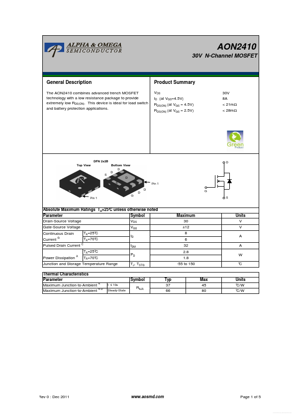
The AON2410 combines advanced trench MOSFET technology with a low resistance package to provide extremely low RDS(ON).
This device is ideal for load switch and battery protection applications.
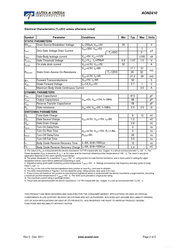
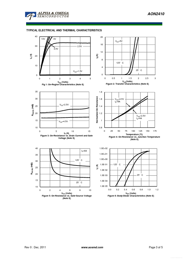
Product Summary VDS ID (at VGS=4.5V) RDS(ON) (at VGS = 4.5V) RDS(ON) (at VGS = 2.5V) 30V 8A < 21mΩ < 28mΩ DFN 2x2B Top View S Bottom View D D D S D Pin 1 G D Pin 1 G D S Absolute Maximum Ratings TA=25° C unless otherwise noted Parameter Symbol Drain-Source Voltage VDS Gate-Source Voltage Continuous Drain Current G Pulsed Drain Current C TA=25° C Power Dissipation A TA=70° C Junction and Storage Temperature Range Thermal Characteristics Parameter Maximum Junction-to-Ambient A Maximum Junction-to-Ambient A D TA=25° C TA=70° C VGS ID IDM PD TJ, TSTG Maximum 30 ±12 8 6 32 2.8 1.8 -55 to 150 Units V V A A W ° C Symbol t ≤ 10s Steady-State RθJA Typ 37 66 Max 45 80 Units ° C/W ° C/W Rev 0 : Dec 2011 www.aosmd.com Page 1 of 5 Free Datasheet http://www.datasheet4u.com/ AON2410 Electrical Characteristics (TJ=25° C unless otherwise noted) Symbol Parameter Conditions ID=250µA, VGS=0V VDS=30V, VGS=0V C TJ=55° VDS=0V, VGS=±12V VDS=VGS,ID=250µA VGS=4.5V, VDS=5V VGS=4.5V, ID=8A RDS(ON) gFS VSD IS Static Drain-Source On-Resistance VGS=2.5V, ID=4A Forward Transconductance Diode Forward Voltage VDS=5V, ID=8A IS=1A,VGS=0V TJ=125° C 0.6 32 17.1 26 21.2 50 0.7 1 3.5 813 VGS=0V, VDS=15V, f=1MHz VGS=0V, VDS=0V, f=1MHz 98 56 2.3 8 VGS=4.5V, VDS=15V, ID=8A 1.2 2.6 3 VGS=4.5V, VDS=15V, RL=1.8Ω, RGEN=3Ω IF=8A, dI/dt=100A/µs 3 26 3.5 10 2.4 3.5 12 21 32 28 1.07 Min 30 1 5 ±100 1.5 Typ Max Units V µA nA V A mΩ mΩ S V A pF pF pF Ω nC nC nC ns ns ns ns ns nC STATIC PARAMETERS Drain-Source Breakdown Voltage BVDSS IDSS IGSS VGS(th) ID(ON) Zero Gate Voltage Drain Current Gate-Body leakage current Gate Threshold Voltage On state drain current Maximum Body-Diode Continuous Current DYNAMIC PARAMETERS Ciss Input Capacitance Coss Crss Rg Output C
| Part Number | Description |
|---|---|
| AON2411 | 12V P-Channel MOSFET |
| AON2400 | 8V N-Channel MOSFET |
| AON2401 | 8V P-Channel MOSFET |
| AON2403 | 12V P-Channel MOSFET |
| AON2405 | 20V P-Channel MOSFET |
| AON2406 | 20V N-Channel MOSFET |
| AON2407 | 30V P-Channel MOSFET |
| AON2408 | 20V N-Channel MOSFET |
| AON2409 | 30V P-Channel MOSFET |
| AON2420 | 30V N-Channel AlphaMOS |