Datasheet Details
| Part number | AON6414A |
|---|---|
| Manufacturer | Alpha & Omega Semiconductors |
| File Size | 467.50 KB |
| Description | 30V N-Channel MOSFET |
| Download | AON6414A Download (PDF) |
|
|
| Part number | AON6414A |
|---|---|
| Manufacturer | Alpha & Omega Semiconductors |
| File Size | 467.50 KB |
| Description | 30V N-Channel MOSFET |
| Download | AON6414A Download (PDF) |
|
|
|
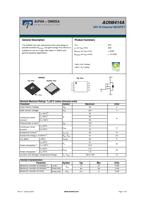
Product Summary The AON6414A uses advanced trench technology to provide excellent RDS(ON), low gate charge.This device is suitable for use as a high side switch in SMPS and general purpose applications.
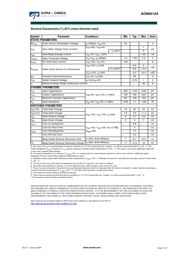
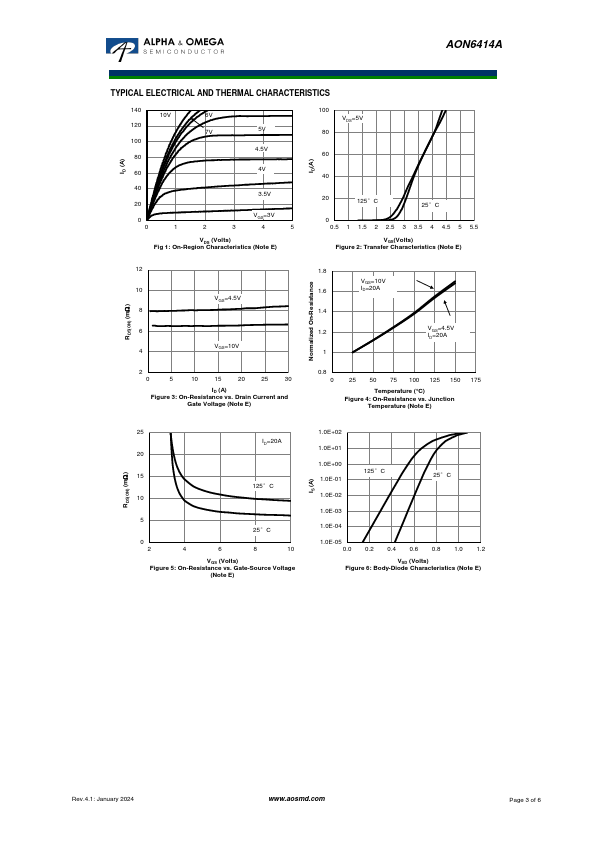
VDS ID (at VGS=10V) RDS(ON) (at VGS=10V) RDS(ON) (at VGS=4.5V) 30V 30A < 8mW < 10.5mW 100% UIS Tested 100% Rg Tested Top View DFN5X6 Bottom View PIN1 Top View S1 S2 S3 G4 8D 7D 6D 5D G Absolute Maximum Ratings TA=25°C unless otherwise noted Parameter Symbol Drain-Source Voltage VDS Gate-Source Voltage VGS TC=25°CG Continuous Drain TC=25°CI ID Current TC=100°C Pulsed Drain Current C IDM Continuous Drain TA=25°C Current TA=70°C Avalanche Current C Avalanche energy L=0.05mH C IDSM IAS, IAR EAS, EAR VDS Spike 100ns VSPIKE TC=25°C Power Dissipation B TC=100°C PD TA=25°C Power Dissipation A TA=70°C PDSM Junction and Storage Temperature Range TJ, TSTG Maximum 30 ±20 30 50 30 140 13 10 35 31 36 31 12.5 2.3 1.5 -55 to 150 Thermal Characteristics Parameter Symbol Typ Maximum Junction-to-Ambient A t ≤ 10s Maximum Junction-to-Ambient A D Steady-State RqJA 17 44 Maximum Junction-to-Case Steady-State RqJC 3.4 Max 21 53 4 D S Units V V A A A mJ V W W °C Units °C/W °C/W °C/W Rev.4.1: January 2024 www.aosmd.com Page 1 of 6 AON6414A Electrical Characteristics (TJ=25°C unless otherwise noted) Symbol Parameter Conditions Min Typ Max Units STATIC PARAMETERS BVDSS Drain-Source Breakdown Voltage ID=250mA, VGS=0V 30 V IDSS Zero Gate Voltage Drain Current VDS=30V, VGS=0V TJ=55°C 1 5 mA IGSS Gate-Body leakage current VDS=0V, VGS= ±20V 100 nA VGS(th) Gate Threshold Voltage VDS=VGS ID=250mA 1.5 1.95 2.5 V ID(ON) On state drain current VGS=10V, VDS=5V 140 A RDS(ON) Static Drain-Source On-Resistance VGS=10V, ID=20A TJ=125°C 6.6 8 9.5 11.4 mW VGS=4.5V, ID=20A 8.2 10.5 mW gFS Forward Transconductance VDS=5V, ID=20A 55 S VSD Diode Forward Volt
AON6414A 30V N-Channel MOSFET General.
| Part Number | Description |
|---|---|
| AON6414 | N-Channel MOSFET |
| AON6410 | N-Channel MOSFET |
| AON6411 | 20V P-Channel MOSFET |
| AON6413 | 30V P-Channel MOSFET |
| AON6416 | N-Channel MOSFET |
| AON6418 | N-Channel MOSFET |
| AON6400 | N-Channel MOSFET |
| AON6403 | 30V P-Channel MOSFET |
| AON6403L | N-Channel MOSFET |
| AON6404 | N-Channel MOSFET |