Datasheet Details
| Part number | AON6850 |
|---|---|
| Manufacturer | Alpha & Omega Semiconductors |
| File Size | 489.45 KB |
| Description | N-Channel MOSFET |
| Download | AON6850 Download (PDF) |
|
|
| Part number | AON6850 |
|---|---|
| Manufacturer | Alpha & Omega Semiconductors |
| File Size | 489.45 KB |
| Description | N-Channel MOSFET |
| Download | AON6850 Download (PDF) |
|
|
|
The AON6850 is fabricated with SDMOSTM trench technology that combines excellent RDS(ON) with low gate charge and low Qrr.The result is outstanding efficiency with controlled switching behavior.
This universal technology is well suited for PWM, load switching and general purpose applications.
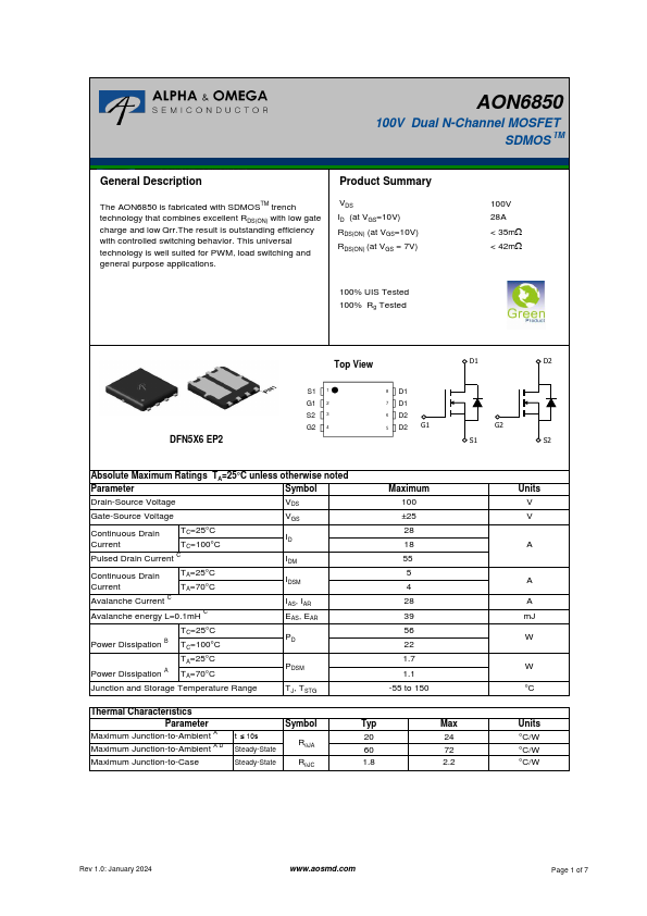
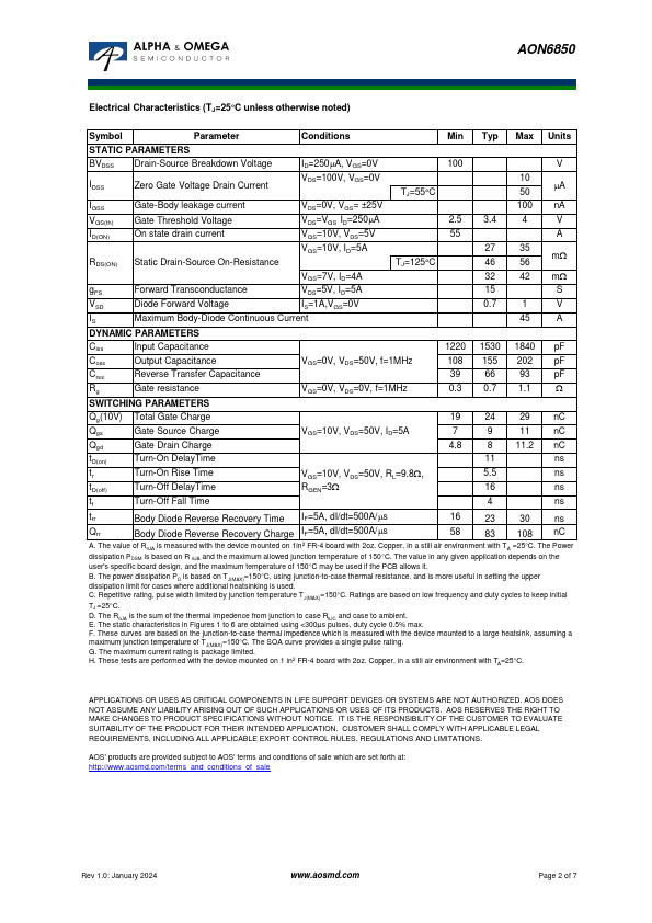
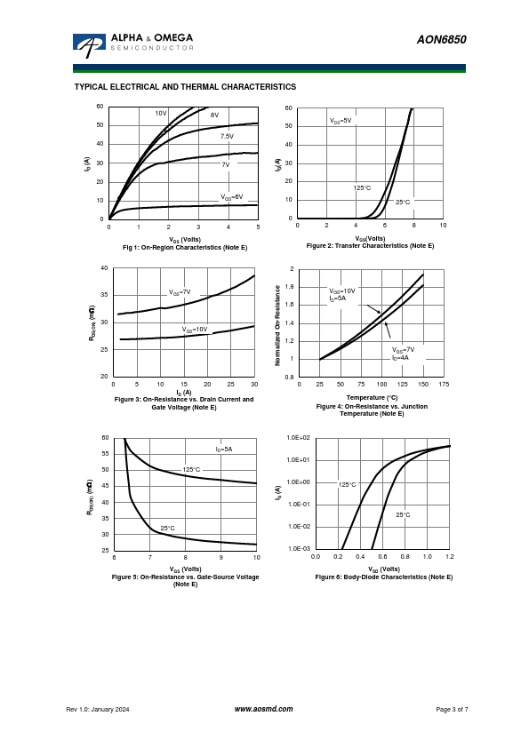
Product Summary VDS ID (at VGS=10V) RDS(ON) (at VGS=10V) RDS(ON) (at VGS = 7V) 100% UIS Tested 100% Rg Tested 100V 28A < 35mW < 42mW DFN5X6 EP2 Top View D1 D2 SS1 1 GS1 2 SS2 3 GG2 4 8 D1 7 D1 6 D2 5 D2 G1 G2 S1 S2 Absolute Maximum Ratings TA=25°C unless otherwise noted Parameter Symbol Drain-Source Voltage VDS Gate-Source Voltage Continuous Drain TC=25°C Current TC=100°C Pulsed Drain Current C Continuous Drain Current Avalanche Current C TA=25°C TA=70°C Avalanche energy L=0.1mH C VGS ID IDM IDSM IAS, IAR EAS, EAR TC=25°C Power Dissipation B TC=100°C PD TA=25°C Power Dissipation A TA=70°C PDSM Junction and Storage Temperature Range TJ, TSTG Maximum 100 ±25 28 18 55 5 4 28 39 56 22 1.7 1.1 -55 to 150 Thermal Characteristics Parameter Symbol Typ Maximum Junction-to-Ambient A t ≤ 10s Maximum Junction-to-Ambient A D Steady-State RqJA 20 60 Maximum Junction-to-Case Steady-State RqJC 1.8 Max 24 72 2.2 Units V V A A A mJ W W °C Units °C/W °C/W °C/W Rev 1.0: January 2024 www.aosmd.com Page 1 of 7 AON6850 Electrical Characteristics (TJ=25°C unless otherwise noted) Symbol Parameter Conditions Min Typ Max Units STATIC PARAMETERS BVDSS Drain-Source Breakdown Voltage ID=250mA, VGS=0V 100 V IDSS Zero Gate Voltage Drain Current VDS=100V, VGS=0V TJ=55°C 10 50 mA IGSS Gate-Body leakage current VDS=0V, VGS= ±25V 100 nA VGS(th) Gate Threshold Voltage VDS=VGS ID=250mA 2.5 3.4 4 V ID(ON) On state drain current VGS=10V, VDS=5V 55 A RDS(ON) Static Drain-Source On-Resistance VGS=10V, ID=5A TJ=125°C 27 35 46 56 mW VGS=7V, ID=4A 32 42 mW gFS
AON6850 100V Dual N-Channel MOSFET SDMOS TM General.
| Part Number | Description |
|---|---|
| AON6810 | N-Channel MOSFET |
| AON6812 | 30V Common Drain N-Channel MOSFET |
| AON6816 | 30V Dual N-Channel MOSFET |
| AON6884 | N-Channel MOSFET |
| AON6144 | 40V N-Channel MOSFET |
| AON6152A | 45V N-Channel MOSFET |
| AON6154 | 45V N-Channel MOSFET |
| AON6156 | 45V N-Channel MOSFET |
| AON6160 | N-Channel MOSFET |
| AON6162 | 60V N-Channel MOSFET |