AONV070V65G1 650V Enhancement Mode GaN Transistor Features 650V Enhancement Mode GaN Transistor Normal-off Design Ultra-low Qg No Qrr Low Inductance Application...
View more extracted text
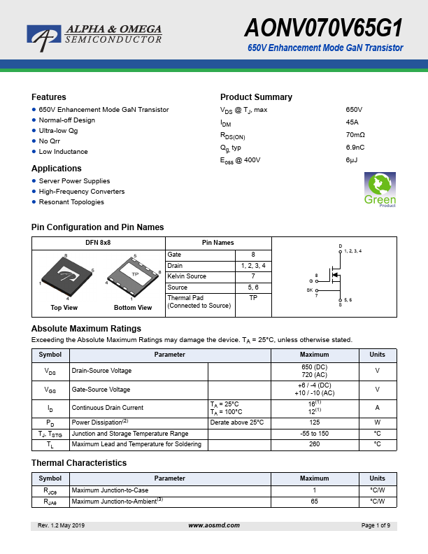
Normal-off Design Ultra-low Qg No Qrr Low Inductance Applications Server Power Supplies High-Frequency Converters Resonant Topologies Product Summary VDS @ TJ, max IDM RDS(ON) Qg, typ Eoss @ 400V 650V 45A 70mΩ 6.9nC 6µJ Pin Configuration and Pin Names DFN 8x8 Top View Bottom View Pin Names Gate Drain Kelvin Source Source Thermal Pad (Connected to Source) 8 1, 2, 3, 4 7 5, 6 TP D 1, 2, 3, 4 8 G SK 7 5, 6 S Absolute Maximum Ratings Exceeding the Absolute Maximum Ratings may damage the device. TA = 25°C, unless otherwise stated.
 AONV070V65G1 Datasheet