Datasheet Details
| Part number | AONV110A60 |
|---|---|
| Manufacturer | Alpha & Omega Semiconductors |
| File Size | 500.39 KB |
| Description | N-Channel Power Transistor |
| Datasheet | AONV110A60-AlphaOmegaSemiconductors.pdf |
|
|
Overview: AONV110A60 600V, a MOS5 TM N-Channel Power Transistor General.
| Part number | AONV110A60 |
|---|---|
| Manufacturer | Alpha & Omega Semiconductors |
| File Size | 500.39 KB |
| Description | N-Channel Power Transistor |
| Datasheet | AONV110A60-AlphaOmegaSemiconductors.pdf |
|
|
|
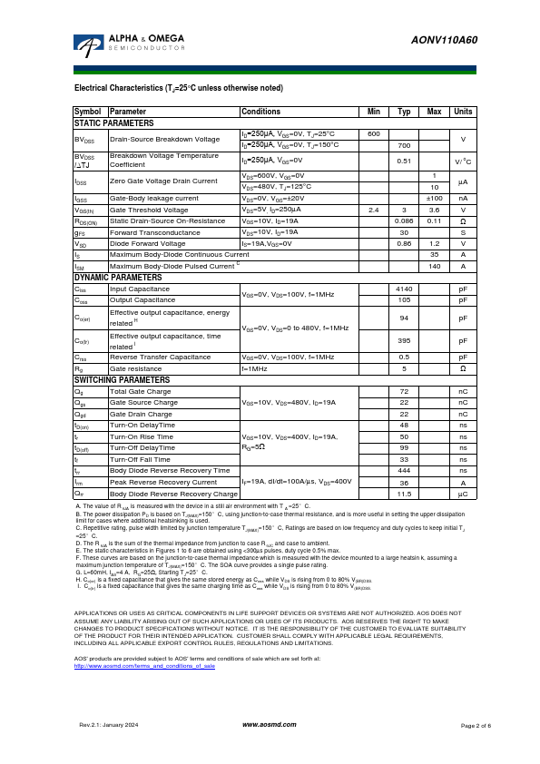
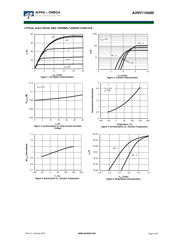
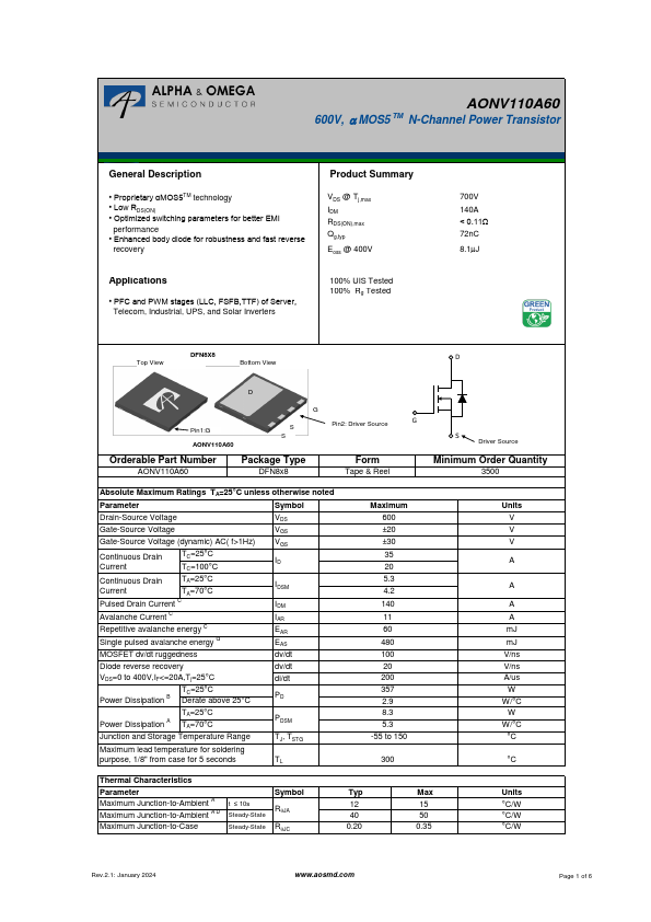
• Proprietary αMOS5TM technology • Low RDS(ON) • Optimized switching parameters for better EMI performance • Enhanced body diode for robustness and fast reverse recovery Product Summary VDS @ Tj,max IDM RDS(ON),max Qg,typ Eoss @ 400V Applications • PFC and PWM stages (LLC, FSFB,TTF) of Server, Telecom, Industrial, UPS, and Solar Inverters 100% UIS Tested 100% Rg Tested 700V 140A < 0.11Ω 72nC 8.1mJ DFN8X8 D Top View Bottom View D G Pin1:G AONV110A60 S S Orderable Part Number AONV110A60 Package Type DFN8x8 Pin2: Driver Source Form Tape & Reel G S Driver Source Minimum Order Quantity 3500 Absolute Maximum Ratings TA=25°C unless otherwise noted Parameter Symbol Drain-Source Voltage VDS Gate-Source Voltage VGS Gate-Source Voltage (dynamic) AC( f>1Hz) VGS Continuous Drain Current TC=25°C TC=100°C ID Continuous Drain TA=25°C Current TA=70°C Pulsed Drain Current C Avalanche Current C Repetitive avalanche energy C Single pulsed avalanche energy G MOSFET dv/dt ruggedness IDSM IDM IAR EAR EAS dv/dt Diode reverse recovery dv/dt VDS=0 to 400V,IF<=20A,Tj=25°C di/dt TC=25°C Power Dissipation B Derate above 25°C PD TA=25°C Power Dissipation A TA=70°C PDSM Junction and Storage Temperature Range Maximum lead temperature for soldering purpose, 1/8" from case for 5 seconds TJ, TSTG TL Maximum 600 ±20 ±30 35 20 5.3 4.2 140 11 60 480 100 20 200 357 2.9 8.3 5.3 -55 to 150 300 Units V V V A A A A mJ mJ V/ns V/ns A/us W W/°C W W/°C °C °C Thermal Characteristics Parameter Maximum Junction-to-Ambient A Maximum Junction-to-Ambient A D Maximum Junction-to-Case t ≤ 10s Steady-State Steady-State Symbol RqJA RqJC Typ 12 40 0.20 Max 15 50 0.35 Units °C/W °C/W °C/W Rev.2.1: January 2024 www.aosmd.com Page 1 of 6 AONV110A60 Electrical Characteristics (TJ=25°C unless otherwise noted) Symbol Parameter Conditions Min Typ Max Units STATIC PARAMETERS BVDSS BVDSS /∆TJ I
| Part Number | Description |
|---|---|
| AONV125A60 | N-Channel Power Transistor |
| AONV140A60 | N-Channel Power Transistor |
| AONV180A60 | N-Channel Power Transistor |
| AONV070V65G1 | 650V Enhancement Mode GaN Transistor |
| AONV210A60 | N-Channel Power Transistor |
| AONV310A60 | N-Channel Power Transistor |
| AONV420A60 | N-Channel Power Transistor |
| AONV420A70 | N-Channel Power Transistor |
| AON1605 | 20V P-Channel MOSFET |
| AON1606 | 20V N-Channel MOSFET |