The following content is an automatically extracted verbatim text
from the original manufacturer datasheet and is provided for reference purposes only.
View original datasheet text
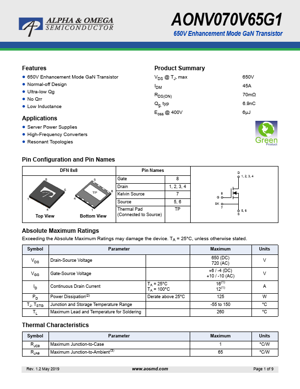
AONV070V65G1
650V Enhancement Mode GaN Transistor
Features
650V Enhancement Mode GaN Transistor Normal-off Design Ultra-low Qg No Qrr Low Inductance
Applications
Server Power Supplies High-Frequency Converters Resonant Topologies
Product Summary
VDS @ TJ, max IDM RDS(ON) Qg, typ Eoss @ 400V
650V 45A 70mΩ 6.9nC 6µJ
Pin Configuration and Pin Names
DFN 8x8
Top View
Bottom View
Pin Names
Gate Drain
Kelvin Source Source Thermal Pad (Connected to Source)
8 1, 2, 3, 4
7 5, 6 TP
D 1, 2, 3, 4
8 G
SK 7
5, 6 S
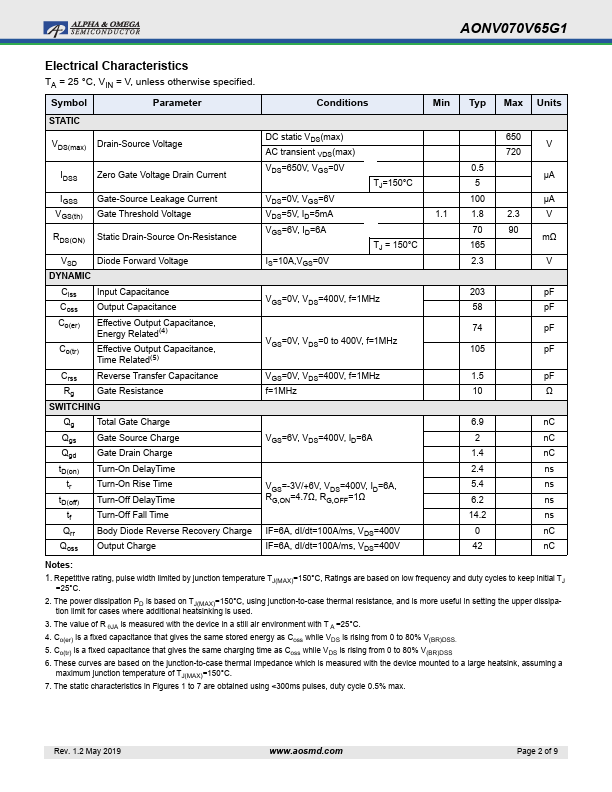
Absolute Maximum Ratings
Exceeding the Absolute Maximum Ratings may damage the device. TA = 25°C, unless otherwise stated.
 AONV070V65G1 Datasheet