• Part: ADG5412BF
  • Description: Quad SPST Switches
  • Manufacturer: Analog Devices
  • Size: 710.71 KB
Download ADG5412BF Datasheet PDF
Analog Devices
ADG5412BF
ADG5412BF is Quad SPST Switches manufactured by Analog Devices.
FEATURES Overvoltage protection up to - 55 V and +55 V Power-off protection up to - 55 V and +55 V Overvoltage detection on source and drain pins Low on resistance: 10 Ω On-resistance flatness of 0.5 Ω 3 k V human body model (HBM) ESD rating Latch-up immune under any circumstance Known state without digital inputs present VSS to VDD analog signal range ±5 V to ±22 V dual-supply operation 8 V to 44 V single-supply operation Fully specified at ±15 V, ±20 V, +12 V, and +36 V APPLICATIONS Analog input/output modules Process control/distributed control systems Data acquisition Instrumentation Avionics Automatic test equipment munication systems Relay replacement GENERAL DESCRIPTION 
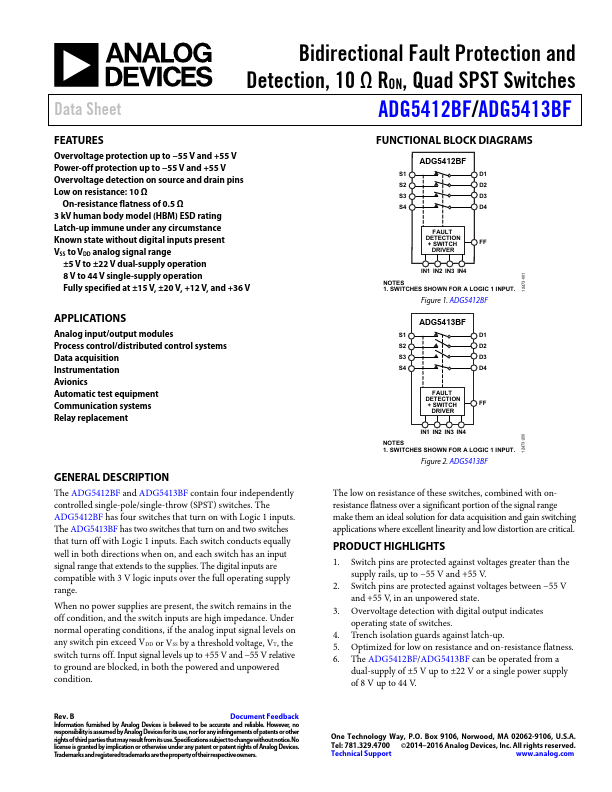
The ADG5412BF and ADG5413BF contain four independently controlled single-pole/single-throw (SPST) switches. The ADG5412BF has four switches that turn on with Logic 1 inputs. The ADG5413BF has two switches that turn on and two switches that turn off with Logic 1 inputs. Each switch conducts equally well in both directions when on, and each switch has an input signal range that extends to the supplies. The digital inputs are patible with 3 V logic inputs over the full operating supply range. When no power supplies are present, the switch remains in the off condition, and the switch inputs are high impedance. Under normal operating conditions, if the analog input signal levels on any switch pin exceed VDD or VSS by a threshold voltage, VT, the switch turns off. Input signal levels up to +55 V and - 55 V relative to ground are blocked, in both the powered and unpowered condition. FUNCTIONAL BLOCK DIAGRAMS S1 D1 S2 D2 S3 D3 S4 D4 12473-001 FAULT DETECTION + SWITCH DRIVER IN1 IN2 IN3 IN4 NOTES 1. SWITCHES SHOWN FOR A LOGIC 1 INPUT. Figure 1. ADG5412BF ADG5413BF S1 D1 S2 D2 S3 D3 S4 D4 FAULT DETECTION + SWITCH DRIVER IN1 IN2 IN3 IN4 NOTES 1. SWITCHES SHOWN FOR A LOGIC 1 INPUT. Figure 2. ADG5413BF 12473-200 The low on resistance of these switches, bined with onresistance...