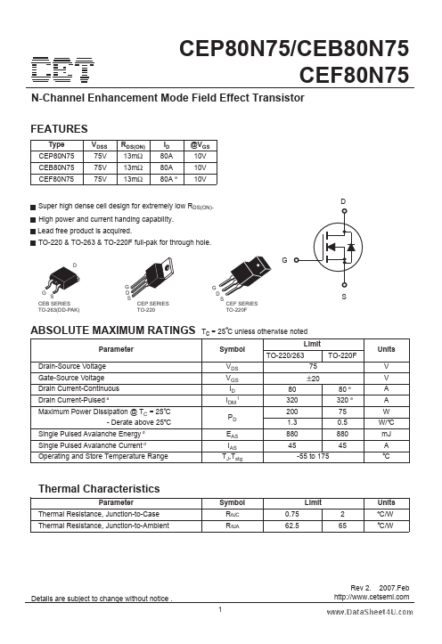
CEP80N75/CEB80N75
CEF80N75
Electrical Characteristics Tc = 25 C unless otherwise noted
Parameter
Off Characteristics
Drain-Source Breakdown Voltage
Zero Gate Voltage Drain Current
Gate Body Leakage Current, Forward
Gate Body Leakage Current, Reverse
On Characteristics b
Symbol
Test Condition
BVDSS
IDSS
IGSSF
IGSSR
VGS = 0V, ID = 250µA
VDS = 60V, VGS = 0V
VGS = 20V, VDS = 0V
VGS = -20V, VDS = 0V
Gate Threshold Voltage
Static Drain-Source
On-Resistance
VGS(th)
RDS(on)
VGS = VDS, ID = 250µA
VGS = 10V, ID = 40A
Dynamic Characteristics c
Forward Transconductance
Input Capacitance
Output Capacitance
Reverse Transfer Capacitance
Switching Characteristics c
gFS
Ciss
Coss
Crss
VDS = 15V, ID = 40A
VDS = 25V, VGS = 0V,
f = 1.0 MHz
Turn-On Delay Time
Turn-On Rise Time
Turn-Off Delay Time
td(on)
tr
td(off)
VDD = 37.5V, ID = 45A,
VGS = 10V, RGEN = 4.7Ω
Turn-Off Fall Time
tf
Total Gate Charge
Gate-Source Charge
Gate-Drain Charge
Qg
Qgs
VDS = 60V, ID = 75A,
VGS = 10V
Qgd
Drain-Source Diode Characteristics and Maximun Ratings
Drain-Source Diode Forward Current
Drain-Source Diode Forward Voltage b
IS g
VSD
VGS = 0V, IS = 75A
Notes :
a.Repetitive Rating : Pulse width limited by maximum junction temperature .
b.Pulse Test : Pulse Width < 300µs, Duty Cycle < 2% .
c.Guaranteed by design, not subject to production testing.
d.L =0.87mH, IAS =45A, VDD = 38V, RG = 25Ω, Starting TJ = 25 C .
e.Limited only by maximum temperature allowed .
f .Pulse width limited by safe operating area .
g.Full package IS(max) = 51A .
Min
75
2
Typ Max Units
1
100
-100
V
µA
nA
nA
4V
10 13 mΩ
45
3550
580
40
S
pF
pF
pF
24 48
5 10
61 122
18 36
79.3 105.5
20.6
25.9
ns
ns
ns
ns
nC
nC
nC
75 A
1.5 V
2