CEC8218
CEC8218 is Dual N-Channel MOSFET manufactured by CET.
Dual N-Channel Enhancement Mode Field Effect Transistor
Features
20V, 7A, RDS(ON) = 20mΩ @VGS = 4.5V. RDS(ON) = 28mΩ @VGS = 2.5V. RDS(ON) = 48mΩ @VGS = 1.8V.
Super High dense cell design for extremely low RDS(ON). High power and current handing capability. Lead free product is acquired.
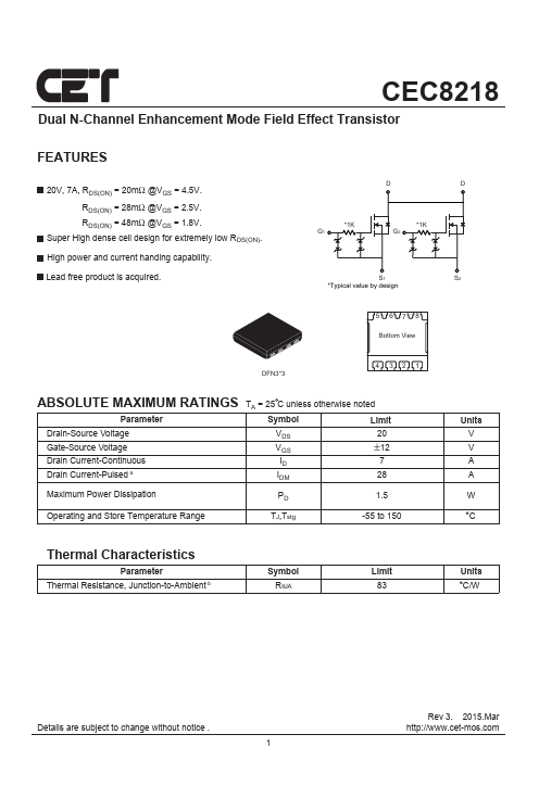
- 1K G1
- 1K G2
S1
- Typical value by design
5 67 8 Bottom View
DFN3- 3
4...