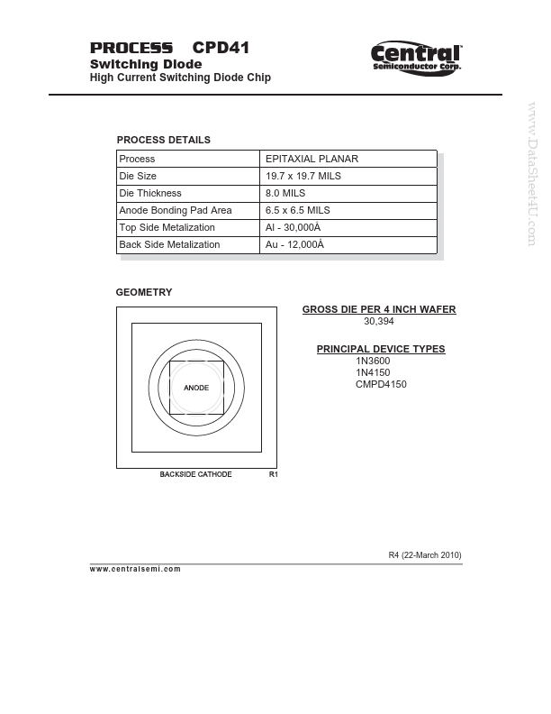
CPD41 Description
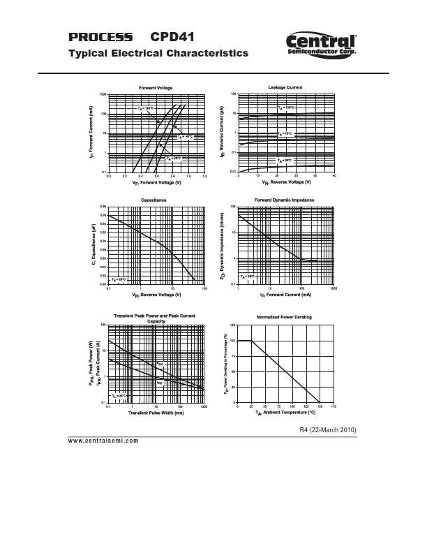
PROCESS CPD41 Switching Diode High Current Switching Diode Chip .. c o m PROCESS CPD41 Typical R4 (22-March 2010) w w.
CPD41 Key Features
- s e m i . c o m PROCESS CPD41 Typical
CPD41 is Switching Diode High Current Switching Diode manufactured by Central Semiconductor.
| Part Number | Description |
|---|---|
| CPD48V | Schottky Diode High Current Schottky Diode |
| CPD04 | 500mA Glass Passivated Rectifier |
| CPD05 | 1 Amp Glass Passivated Rectifier |
| CPD06 | 3 Amp Glass Passivated Rectifier |
| CPD15 | 500mA Glass Passivated Rectifier |
PROCESS CPD41 Switching Diode High Current Switching Diode Chip .. c o m PROCESS CPD41 Typical R4 (22-March 2010) w w.