CY23S09 Overview
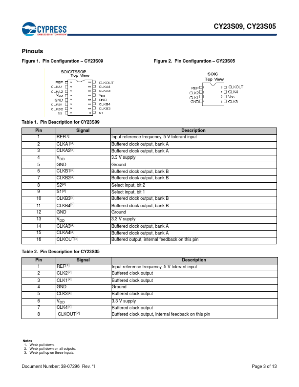
The CY23S09 is a low cost 3.3 V zero delay buffer designed to distribute high speed clocks and is available in a 16-pin SOIC package. The CY23S05 is an 8-pin version of the CY23S09. It accepts one reference input, and drives.
CY23S09 Key Features
- 10 MHz to 100 MHz and 133 MHz operating range, patible with CPU and PCI bus frequencies
- Zero input-output propagation delay
- Multiple low skew outputs
- Output-output skew less than 250 ps
- Device-device skew less than 700 ps
- One input drives five outputs (CY23S05)
- One input drives nine outputs, grouped as 4 + 4 + 1 (CY23S09)
- Less than 200 ps Cycle-to-cycle jitter
- Test mode to bypass PLL (CY23S09 only, see Select Input Decoding for CY23S09 on page 4)
- 3.3 V operation, advanced 0.65 CMOS technology