Datasheet4U Logo Datasheet4U.com

CY2302

Frequency Multiplier and Zero Delay Buffer

CY2302 Features

* 90 ps typical jitter OUT2

* 200 ps typical jitter OUT1

* 65 ps typical output-to-output skew

* 90 ps typical propagation delay

* Voltage range: 3.3 V±5%, or 5 V±10%

* Output frequency range: 5 MHz to 133 MHz

* Two outputs

* Configuration options allow various multip

CY2302 General Description

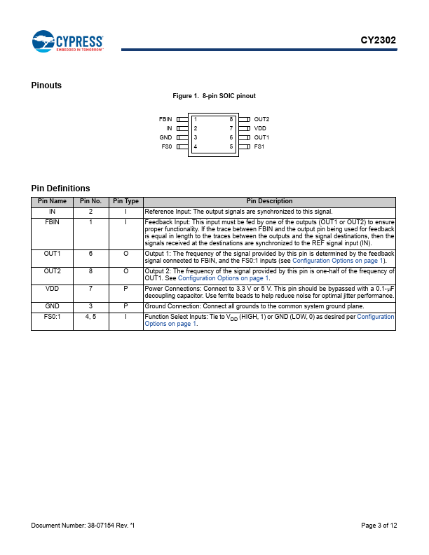
Reference Input: The output signals are synchronized to this signal. Feedback Input: This input must be fed by one of the outputs (OUT1 or OUT2) to ensure proper functionality. If the trace between FBIN and the output pin being used for feedback is equal in length to the traces between the outputs a.

CY2302 Datasheet (323.60 KB)

Preview of CY2302 PDF

Datasheet Details

Part number:

CY2302

Manufacturer:

Cypress Semiconductor

File Size:

323.60 KB

Description:

Frequency multiplier and zero delay buffer.

📁 Related Datasheet

CY2300 Phase-Aligned Clock Multiplier (Cypress Semiconductor)

CY2303 Phase-Aligned Clock Multiplier (Cypress Semiconductor)

CY2304 3.3V Zero Delay Buffer (Cypress)

CY2304NZ Four Output PCI-X and General Purpose Buffer (Cypress)

CY2305 Low Cost 3.3 V Zero Delay Buffer (Cypress)

CY2305C Zero Delay Buffers (Cypress Semiconductor)

CY2308 3.3V Zero Delay Buffer (Cypress)

CY2309 Low Cost 3.3 V Zero Delay Buffer (Cypress)

CY2309C Zero Delay Buffers (Cypress Semiconductor)

CY2313ANZ 3.3V SDRAM Buffer for Desktop PCs with 3 DIMMs (Cypress Semiconductor)

TAGS

CY2302 Frequency Multiplier and Zero Delay Buffer Cypress Semiconductor

Image Gallery

CY2302 Datasheet Preview Page 2 CY2302 Datasheet Preview Page 3

CY2302 Distributor