Datasheet Details
| Part number | CY23EP05 |
|---|---|
| Manufacturer | Cypress |
| File Size | 599.66 KB |
| Description | 5 Output Zero Delay Buffer |
| Datasheet |
 CY23EP05 Datasheet CY23EP05 Datasheet
|
|
|
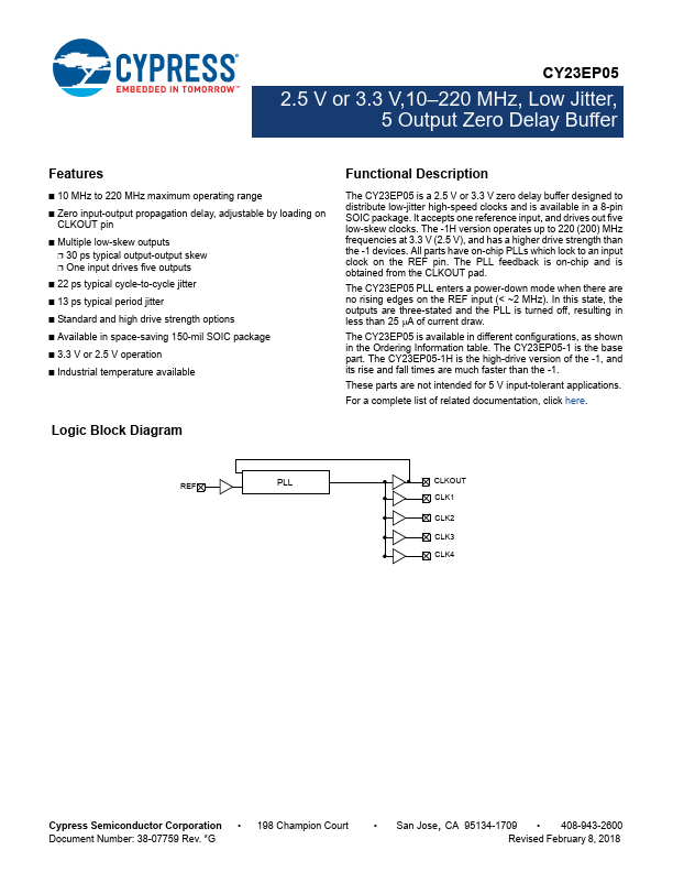
The CY23EP05 is a 2.5 V or 3.3 V zero delay buffer designed to distribute low-jitter high-speed clocks and is available in a 8-pin SOIC package.
It accepts one reference input, and drives out five low-skew clocks.
| Part number | CY23EP05 |
|---|---|
| Manufacturer | Cypress |
| File Size | 599.66 KB |
| Description | 5 Output Zero Delay Buffer |
| Datasheet |
CY23EP05 Datasheet
|
|
|
|