MTB115P10KJ3
MTB115P10KJ3 is P-Channel Enhancement Mode Power MOSFET manufactured by Cystech Electonics.
Spec. No. : C891J3
CYStech Electronics Corp.
Issued Date : 2016.12.23 Revised Date :
P-Channel Enhancement Mode Power MOSFET
Features
- Low Gate Charge
- Simple Drive Requirement
- ESD Protected Gate
- Pb-free Lead Plating & Halogen-free Package
BVDSS ID@VGS=-10V, TC=25°C
RDS(ON)@VGS=-10V, ID=-10A
RDS(ON)@VGS=-4.5V, ID=-8A
-100V -15A 82mΩ(typ) 107mΩ(typ)
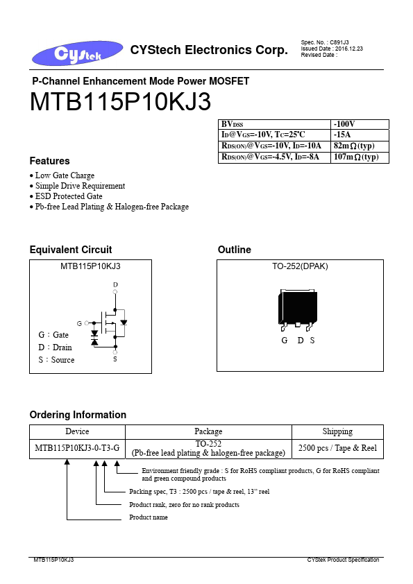
Equivalent Circuit
Outline
TO-252(DPAK)
G:Gate D:Drain S:Source
G DS
Ordering Information
Device MTB115P10KJ3-0-T3-G
Package
TO-252 (Pb-free lead plating & halogen-free package)
Shipping 2500 pcs / Tape & Reel
Environment friendly grade : S for RoHS pliant products, G for RoHS pliant and...