DMN1032UCB4
Description
This 2nd generation Lateral MOSFET (LD-MOS) is engineered to minimize on-state losses and switch ultra-fast, making it ideal for high efficiency power transfer. It uses Chip-Scale Package (CSP) to increase power density by combining low thermal impedance with minimal RDS(ON) per footprint area.
Key Features
- LD-MOS Technology with the Lowest Figure of Merit: RDS(ON) = 18mΩ to Minimize On-State Losses Qg = 3.2nC for Ultra-Fast Switching
- VGS(th) = 0.8V Typ. for a Low Turn-On Potential
- CSP with Footprint 1.0mm × 1.0mm
- Height = 0.62mm for Low Profile
- Totally Lead-Free & Fully RoHS Compliant (Notes 1 & 2)
- Halogen and Antimony Free. “Green” Device (Note 3)
- For automotive applications requiring specific change control (i.e.: parts qualified to AEC-Q100/101/104/200, PPAP capable, and manufactured in IATF 16949 certified facilities), please refer to the related automotive grade (Qsuffix) part. A listing can be found at
- This part is qualified to JEDEC standards (as references in AEC-Q) for High Reliability. Mechanical Data
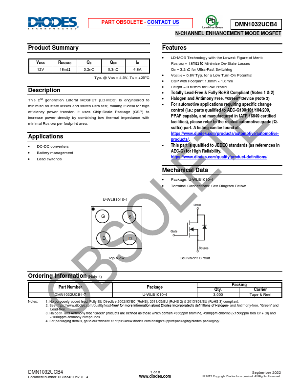
- Package: U-WLB1010-4
- Terminal Connections: See Diagram Below