DFB30N06
DFB30N06 is N-Channel MOSFET manufactured by DnI.
Features
- -
- -
- -
Low RDS(on) (0.04Ω )@VGS=10V Low Gate Charge (Typical 27n C) Low Crss (Typical 75p F) Improved dv/dt Capability 100% Avalanche Tested Maximum Junction Temperature Range
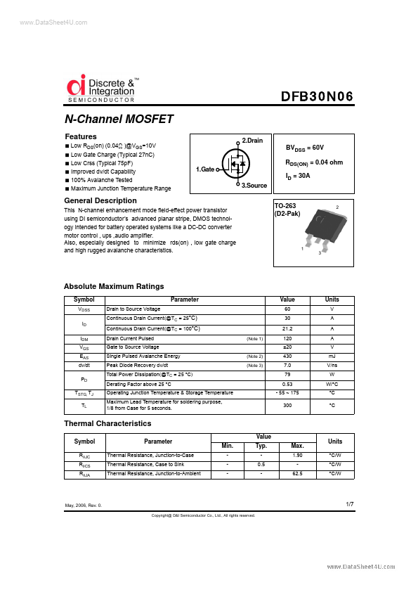
2.Drain
BVDSS = 60V
1.Gate 3.Source
RDS(ON) = 0.04 ohm ID = 30A
General Description
This N-channel enhancement mode field-effect power transistor using DI semiconductor’s advanced planar stripe, DMOS technology intended for battery operated systems like a DC-DC converter motor control , ups ,audio amplifier. Also, especially designed to minimize rds(on) , low gate charge and high rugged avalanche characteristics.
TO-263 (D2-Pak)
Absolute Maximum Ratings
Symbol
VDSS ID IDM VGS EAS dv/dt PD TSTG, TJ TL Drain to Source Voltage Continuous Drain Current(@TC = 25°C) Continuous Drain Current(@TC = 100°C) Drain Current Pulsed Gate to Source Voltage Single Pulsed Avalanche Energy Peak Diode Recovery dv/dt Total Power Dissipation(@TC = 25 °C) Derating Factor above 25 °C Operating Junction Temperature & Storage Temperature Maximum Lead Temperature for soldering purpose, 1/8 from Case for 5 seconds.
(Note 2) (Note 3) (Note 1)
Parameter
Value
60 30 21.2 120 ±20 430 7.0 79 0.53
- 55 ~ 175 300
Units
V A A A V m J V/ns W W/°C °C °C
Thermal Characteristics
Symbol
RθJC RθCS RθJA
Parameter
Thermal Resistance, Junction-to-Case Thermal Resistance, Case to Sink Thermal Resistance, Junction-to-Ambient
Value Min.
- Typ.
- Max.
1.90 62.5
Units
°C/W °C/W °C/W
May, 2006, Rev. 0.
Copyright@ D&I Semiconductor Co., Ltd., All rights...