Datasheet4U Logo Datasheet4U.com

M15F5121632A Datasheet DDR3 SDRAM

Manufacturer: ESMT (Elite Semiconductor Microelectronics Technology)

General Description

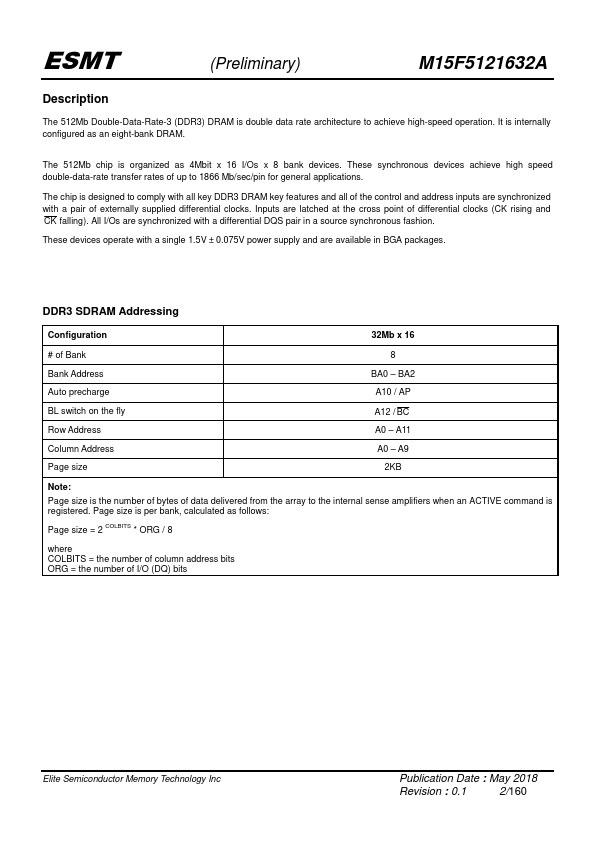
The 512Mb Double-Data-Rate-3 (DDR3) DRAM is double data rate architecture to achieve high-speed operation.

It is internally configured as an eight-bank DRAM.

The 512Mb chip is organized as 4Mbit x 16 I/Os x 8 bank devices.

Overview

ESMT DDR3 SDRAM (Preliminary) Feature Interface and Power Supply ˗ SSTL_15: VDD/VDDQ = 1.5V(±0.075V) JEDEC DDR3 Compliant ˗ 8n Prefetch Architecture ˗ Differential Clock (CK/ CK ) and Data Strobe (DQS/ DQS ) ˗ Double-data rate on DQs, DQS and DM Data Integrity ˗ Auto Refresh and Self Refresh Modes Power Saving Mode ˗ Partial Array Self Refresh(PASR) ˗ Power Down Mode Signal Integrity ˗ Configurable DS for system compatibility ˗ Configurable On-Die Termination ˗ ZQ Calibration for DS/ODT impedance accuracy via external ZQ pad (240 ohm ± 1%) Signal Synchronization M15F5121632A 4M x 16 Bit x 8 Banks DDR3 SDRAM ˗ Write Leveling via MR settings ˗ Read Leveling via MPR Programmable Functions ˗ CAS Latency (5/6/7/8/9/10/11/12/13) ˗ CAS Write Latency (5/6/7/8/9) ˗ Additive Latency (0/CL-1/CL-2) ˗ Write Recovery Time (5/6/7/8/10/12/14/16) ˗ Burst Type (Sequential/Interleaved) ˗ Burst Length (BL8/BC4/BC4 or 8 on the fly) ˗ Self Refresh Temperature Range(Normal/Extended) ˗ Output Driver Impedance (34/40) ˗ On-Die Termination of RTT_Nom(20/30/40/60/120) ˗ On-Die Termination of RTT_WR(60/120) ˗ Precharge Power Down (slow/fast) Ordering Information Product ID Max Freq.

VDD M15F5121632A–EFBG M15F5121632A–DEBG 1066MHz 933MHz 1.5V 1.5V Data Rate (CL-tRCD-tRP) DDR3-2133 (14-14-14) DDR3-1866 (13-13-13) Package Comments 96 ball BGA 96 ball BGA Pb-free Pb-free Elite Semiconductor Memory Technology Inc Publication Date : May 2018 Revision : 0.

Key Features

  • and all of the control and address inputs are synchronized with a pair of externally supplied differential clocks. Inputs are latched at the cross point of differential clocks (CK rising and CK falling). All I/Os are synchronized with a differential DQS pair in a source synchronous fashion. These devices operate with a single 1.5V ± 0.075V power supply and are available in BGA packages. DDR3 SDRAM Addressing Configuration 32Mb x 16 # of Bank 8 Bank Address BA0.
  • BA2 Auto precharg.