XRK32308 Description
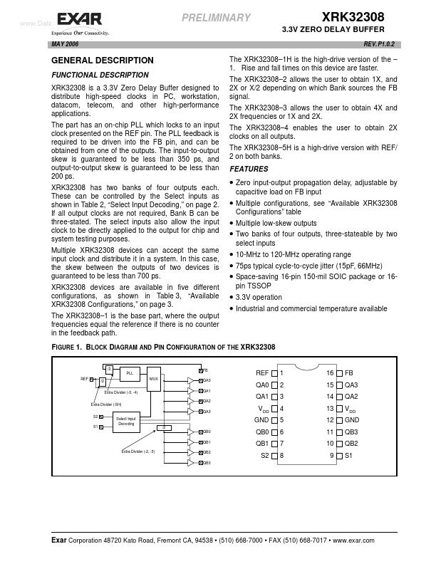
FUNCTIONAL DESCRIPTION XRK32308 is a 3.3V Zero Delay Buffer designed to distribute high-speed clocks in PC, workstation, data, tele, and other high-performance applications. The part has an on-chip PLL which locks to an input clock presented on the REF pin. The PLL feedback is required to be driven into the FB pin, and can be obtained from one of the outputs.
XRK32308 Key Features
- Zero input-output propagation delay, adjustable by
- Multiple configurations, see “Available XRK32308
- Multiple low-skew outputs
- Two banks of four outputs, three-stateable by two
- 10-MHz to 120-MHz operating range
- 75ps typical cycle-to-cycle jitter (15pF, 66MHz)
- Space-saving 16-pin 150-mil SOIC package or 16pin TSSOP
- 3.3V operation
- Industrial and mercial temperature available