XRK32510 Description
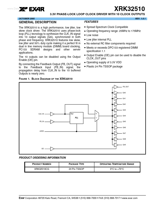
The XRK32510 is a high performance, low jitter, low skew clock driver. The XRK32510 uses phase-lock loop (PLL) tecnology to synthesize the CLK_IN signal into 10 output signals (QA), synchronized in both phase and frequency.
XRK32510 is 3.3V PHASE-LOCK LOOP CLOCK DRIVER manufactured by Exar.
| Part Number | Description |
|---|---|
| XRK32308 | 3.3V ZERO DELAY BUFFER |
| XRK32309 | LOW-COST 3.3V ZERO DELAY BUFFER |
| XRK39351 | 9-OUTPUT PLL CLOCK DRIVER |
| XRK39653 | 8-OUTPUT ZERO DELAY BUFFER |
| XRK39910 | 3.3V LOW SKEW PLL CLOCK DRIVER |
The XRK32510 is a high performance, low jitter, low skew clock driver. The XRK32510 uses phase-lock loop (PLL) tecnology to synthesize the CLK_IN signal into 10 output signals (QA), synchronized in both phase and frequency.