XRK4991
XRK4991 is SKEW CLOCK BUFFER manufactured by Exar.
.. xr
OCTOBER 2005
3.3V HIGH-SPEED (85 MHZ) PROGRAMMABLE SKEW CLOCK BUFFER
REV. 1.0.1
FUNCTIONAL DESCRIPTION
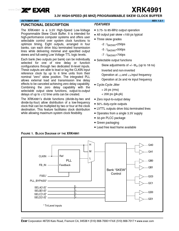
The XRK4991 is a 3.3V High-Speed Low-Voltage Programmable Skew Clock Buffer. It is intended for high-performance puter systems and offers user selectable control over system clock functions to optimize timing. Eight outputs, arranged in four banks, can each drive 50Ω terminated transmission lines while delivering minimal and specified output skews and full-swing Low Voltage TTL logic levels. Each bank (two outputs per bank) can be individually selected for one of nine delay or function configurations through two dedicated tri-level inputs. These outputs are able to lead or lag the CLKIN input reference clock by up to 6 time units from their nominal “zero” skew position. The integrated PLL allows external load and transmission line delay effects to be canceled achieving zero delay capability. bining the zero delay capability with the selectable output skew functions, output-to-output delays of up to ±12 time units can be created. The XRK4991’s divide functions (divide-by-two and divide-by-four) allow distribution of a low-frequency clock that can be multiplied by two or four at the clock destination. This feature facilitates clock distribution while allowing maximum system clock flexibility.
Features
- 3.75- to 85-MHz output operation
- All output pair skew <100 ps typical
- Three skew grades
-2 : t SKEW0<250ps -5 : t SKEW0<500ps -7 : t SKEW0<700ps
- Selectable output functions
Skew adjustments of +/- 6t U (up to 18 ns) Inverted and non-inverted Operation at 1/2 and 1/4 input frequency Operation at 2x and 4x input frequency
- Cycle-Cycle Jitter
< 25 ps (rms) < 200 ps (pk-pk)
- Zero input-to-output delay
- 50% duty-cycle outputs
- LVTTL outputs drive 50Ω terminated lines
- Operates from a single 3.3V supply
- 32-pin PLCC package
- Green packaging
- Lead free lead frame available
FIGURE 1. BLOCK DIAGRAM OF THE XRK4991
H M...