
XRK39653 Description
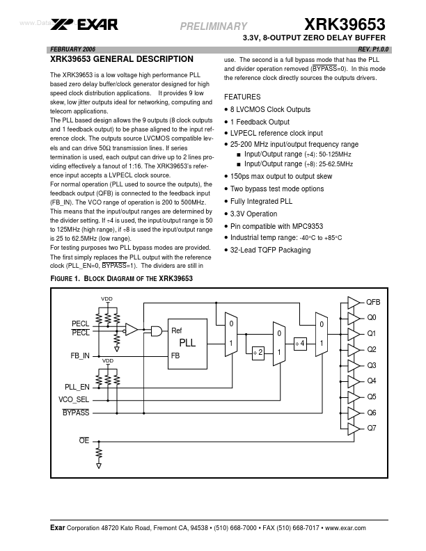
The XRK39653 is a low voltage high performance PLL based zero delay buffer/clock generator designed for high speed clock distribution applications. It provides 9 low skew, low jitter outputs ideal for networking, puting and tele applications. The PLL based design allows the 9 outputs (8 clock outputs and 1 feedback output) to be phase aligned to the input reference clock.
XRK39653 Key Features
- 8 LVCMOS Clock Outputs 1 Feedback Output LVPECL reference clock input 25-200 MHz input/output frequency range
- Input/Output range (÷4): 50-125MHz
- Input/Output range (÷8): 25-62.5MHz
- 150ps max output to output skew
- Two bypass test mode options
- Fully Integrated PLL 3.3V Operation Pin patible with MPC9353 Industrial temp range: -40°C to +85°C 32-Lead TQFP Packagin
- (510) 668-7000
- FAX (510) 668-7017