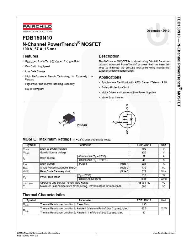
Datasheet Details
| Part number | FDB150N10 |
|---|---|
| Manufacturer | Fairchild (now onsemi) |
| File Size | 574.43 KB |
| Description | N-Channel MOSFET |
| Datasheet | FDB150N10_FairchildSemiconductor.pdf |
|
|
|
Overview: FDB150N10 — N-Channel PowerTrench® MOSFET FDB150N10 N-Channel PowerTrench® MOSFET 100 V, 57 A, 15 mΩ December.
| Part number | FDB150N10 |
|---|---|
| Manufacturer | Fairchild (now onsemi) |
| File Size | 574.43 KB |
| Description | N-Channel MOSFET |
| Datasheet | FDB150N10_FairchildSemiconductor.pdf |
|
|
|
This N-Channel MOSFET is produced using Fairchild Semiconductor’s advanced PowerTrench® process that has been tailored to minimize the on-state resistance while maintaining superior switching performance.
Applications • Synchronous Rectification for ATX / Server / Tele PSU • Battery Protection Circuit • Motor Drives and Uninterruptible Power Supplies • Micro Solar Inverter D D G S D2-PAK G S MOSFET Maximum Ratings TC = 25oC unless otherwise noted.
Symbol VDSS VGSS ID IDM EAS dv/dt PD TJ, TSTG TL Parameter Drain to Source Voltage Gate to Source Voltage Drain Current Drain Current - Continuous (TC = 25oC) - Continuous (TC = 100oC) - Pulsed (Note 1) Single Pulsed Avalanche Energy (Note 2) Peak Diode Recovery dv/dt Power Dissipation (TC = 25oC) - Derate Above 25oC (Note 3) Operating and Storage Temperature Range Maximum Lead Temperature for Soldering, 1/8” from Case for 5 Seconds Thermal Characteristics Symbol RθJC RθJA Parameter Thermal Resistance, Junction to Case, Max.
| Part Number | Description |
|---|---|
| FDB15N50 | N-Channel MOSFET |
| FDB10AN06A0 | N-Channel MOSFET |
| FDB110N15A | MOSFET |
| FDB120N10 | N-Channel MOSFET |
| FDB12N50F | N-Channel MOSFET |
| FDB12N50TM | N-Channel MOSFET |
| FDB12N50U | N-Channel MOSFET |
| FDB13AN06A0 | MOSFET |
| FDB14AN06LA0 | N-Channel MOSFET |
| FDB14N30 | N-Channel MOSFET |