FDMC6686P
Overview
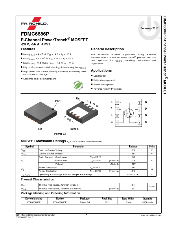
Max rDS(on) = 4 mΩ at VGS = -4.5 V, ID = -18 A Max rDS(on) = 5.7 mΩ at VGS = -2.5 V, ID = -16 A Max rDS(on) =11.5 mΩ at VGS = -1.8 V, ID = -11 A High performance trench technology for extremely low rDS(on) High power and current handling capability in a widely used surface mount package Lead-free and RoHS Compliant This P-Channel MOSFET is produced using Fairchild Semiconductor’s advanced PowerTrench® process that has been optimized for rDS(ON), switching performance and ruggedness.