FDMJ1032C
FDMJ1032C is Dual N & P-Channel PowerTrench MOSFET manufactured by Fairchild Semiconductor.
FDMJ1032C Dual N & P-Channel PowerTrench® MOSFET
Dual N & P-Channel PowerTrench® MOSFET
N-Channel: 20V, 3.2A, 90mΩ P-Channel: -20V, -2.5A, 160mΩ
September 2007 tm
Features
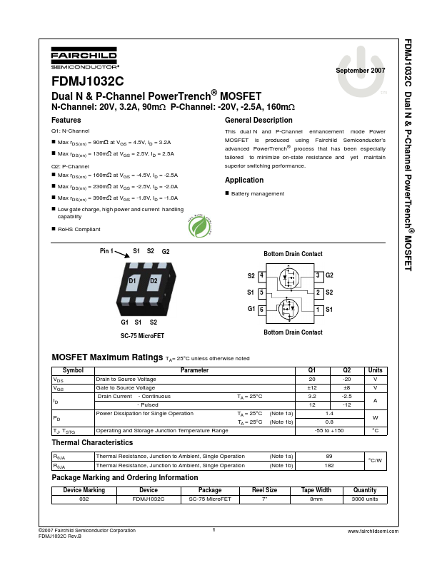
Q1: N-Channel
- Max rDS(on) = 90mΩ at VGS = 4.5V, ID = 3.2A
- Max rDS(on) = 130mΩ at VGS = 2.5V, ID = 2.5A
Q2: P-Channel
- Max rDS(on) = 160mΩ at VGS = -4.5V, ID = -2.5A
- Max rDS(on) = 230mΩ at VGS = -2.5V, ID = -2.0A
- Max rDS(on) = 390mΩ at VGS = -1.8V, ID = -1.0A
- Low gate charge, high power and current handling capability
General Description
This dual N and P-Channel enhancement mode Power MOSFET is produced using Fairchild Semiconductor’s advanced PowerTrench® process that has been especially...