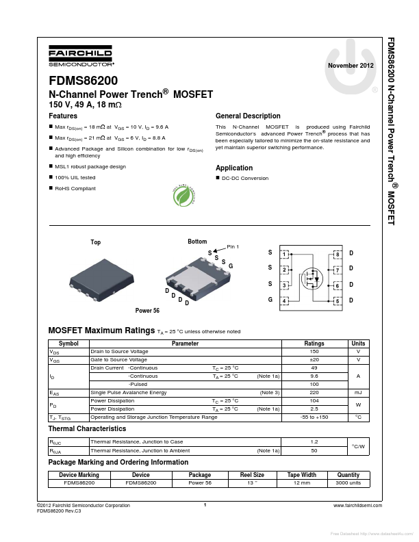
FDMS86200
FDMS86200 is N-Channel MOSFET manufactured by Fairchild Semiconductor.
FDMS86200 N-Channel Power Trench® MOSFET
November 2012
N-Channel Power Trench® MOSFET
150 V, 49 A, 18 mΩ
Features
- Max r DS(on) = 18 mΩ at VGS = 10 V, ID = 9.6 A
- Max r DS(on) = 21 mΩ at VGS = 6 V, ID = 8.8 A
- Advanced Package and Silicon bination for low r DS(on) and high efficiency
- MSL1 robust package design
- 100% UIL tested
- Ro HS pliant
General Description
This N-Channel MOSFET is produced using Fairchild Semiconductor‘s advanced Power Trench® process that has been especially tailored to minimize the on-state resistance and yet maintain superior switching performance.
Application
- DC-DC Conversion
Top
Bottom Pin 1 S S S S G S S D D D G D D D D
Power 56
MOSFET Maximum Ratings TA = 25 °C unless otherwise noted
Symbol VDS VGS ID EAS PD TJ, TSTG Parameter Drain to Source Voltage Gate to Source Voltage Drain Current -Continuous -Continuous -Pulsed Single Pulse Avalanche Energy Power Dissipation Power Dissipation TC = 25 °C TA = 25 °C (Note 1a) (Note 3) TC = 25 °C TA = 25 °C (Note 1a) Ratings 150 ±20 49 9.6 100 220 104 2.5 -55 to +150 m J W °C A Units V V
Operating and Storage Junction Temperature Range
Thermal Characteristics
RθJC RθJA Thermal Resistance, Junction to Case Thermal Resistance, Junction to Ambient (Note 1a) 1.2 50 °C/W
Package Marking and Ordering Information
Device Marking FDMS86200 Device FDMS86200 Package Power 56 Reel Size 13 ’’ Tape Width 12 mm Quantity 3000 units
©2012 Fairchild Semiconductor Corporation FDMS86200 Rev.C3
.fairchildsemi.
Free Datasheet http://../
FDMS86200 N-Channel Power Trench® MOSFET
Electrical Characteristics TJ = 25 °C unless otherwise...