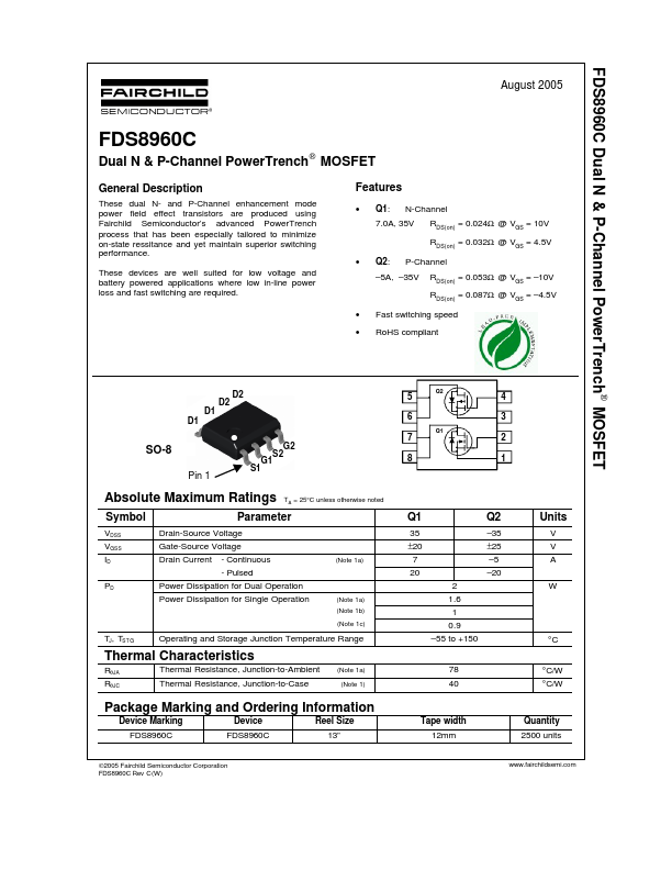
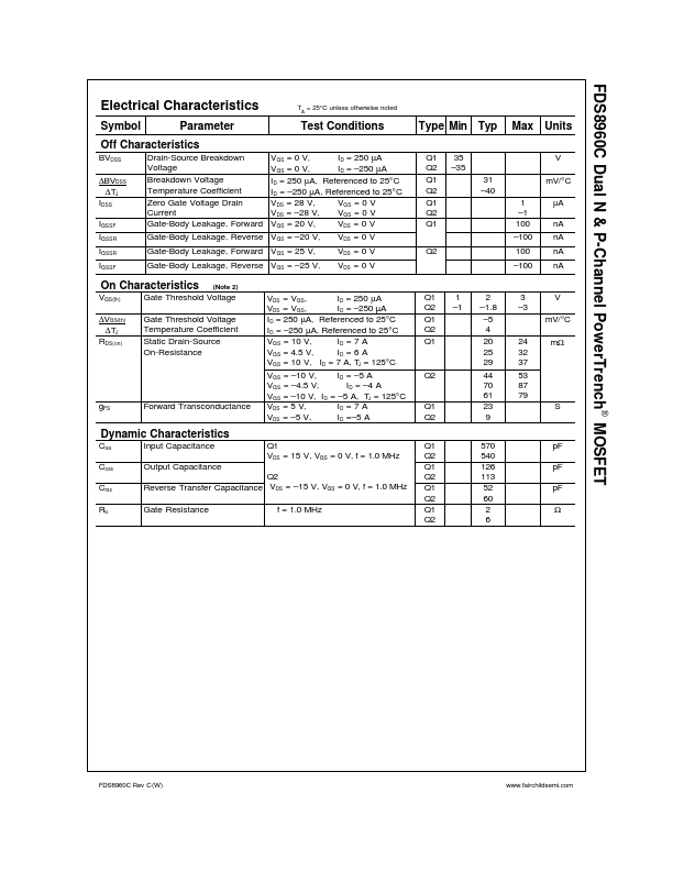
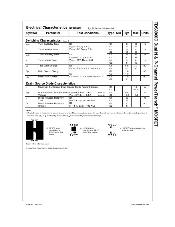
Datasheet4U Logo Datasheet4U.com

FDS8960C - Dual N & P-Channel PowerTrench MOSFET

Description

These dual N- and P-Channel enhancement mode power field effect transistors are produced using Fairchild Semiconductor’s advanced PowerTrench process that has been especially tailored to minimize on-state ressitance and yet maintain superior switching performance.

Features

  • br>.
  • Q1: N-Channel RDS(on) = 0.024Ω @ VGS = 10V RDS(on) = 0.032Ω @ VGS = 4.5V.
  • Q2: P-Channel RDS(on) = 0.053Ω @ VGS =.
  • 10V RDS(on) = 0.087Ω @ VGS =.
  • 4.5V Fast switching speed RoHS compliant 7.0A, 35V.
  • 5A,.
  • 35V D1 D D1 D DD2 D2 D 5 6 7 Q2 4 3 Q1 2 1 SO-8 Pin 1 SO-8 G2 S2 G G1 S S1 S 8 S Absolute Maximum Ratings Symbol VDSS VGSS ID PD Drain-Source Voltage Gate-Source Voltage Drain Current TA = 25°C unless otherwise noted Parameter Q1 35.

📥 Download Datasheet

Datasheet preview – FDS8960C
Other Datasheets by Fairchild Semiconductor

Full PDF Text Transcription

Click to expand full text
www.DataSheet4U.com FDS8960C Dual N & P-Channel PowerTrench® MOSFET August 2005 FDS8960C Dual N & P-Channel PowerTrench® MOSFET General Description These dual N- and P-Channel enhancement mode power field effect transistors are produced using Fairchild Semiconductor’s advanced PowerTrench process that has been especially tailored to minimize on-state ressitance and yet maintain superior switching performance. These devices are well suited for low voltage and battery powered applications where low in-line power loss and fast switching are required. • • Features • Q1: N-Channel RDS(on) = 0.024Ω @ VGS = 10V RDS(on) = 0.032Ω @ VGS = 4.5V • Q2: P-Channel RDS(on) = 0.053Ω @ VGS = –10V RDS(on) = 0.087Ω @ VGS = –4.5V Fast switching speed RoHS compliant 7.
Published: |