FDS8962C
FDS8962C is Dual N & P-Channel PowerTrench MOSFET manufactured by Fairchild Semiconductor.
Features
- Q1: N-Channel 7.0A, 30V RDS(on) = 0.030Ω @ VGS = 10V RDS(on) = 0.044Ω @ VGS = 4.5V
- Q2: P-Channel -5A, -30V RDS(on) = 0.052Ω @ VGS = -10V RDS(on) = 0.080Ω @ VGS = -4.5V
- Fast switching speed
- High power and handling capability in a widely used surface mount package
General Description
These dual N- and P-Channel enhancement mode power field effect transistors are produced using Fairchild Semiconductor’s advanced Power Trench process that has been especially tailored to minimize on-state ressitance and yet maintain superior switching performance. These devices are well suited for low voltage and battery powered applications where low in-line power loss and fast switching are required.
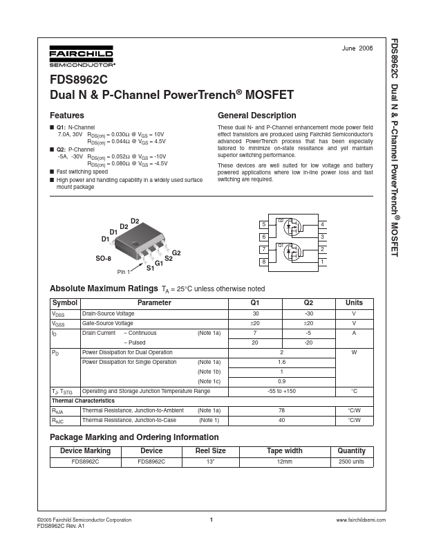
D1 D1
D2
D2
5 6
Q2
4 3
SO-8
Pin 1
S1
G1
G2 S2
7 8
Q1
2 1
Absolute Maximum Ratings TA = 25°C unless otherwise noted
Symbol
VDSS VGSS ID PD Drain-Source Voltage Gate-Source Voltage Drain Current
- Continuous
- Pulsed Power Dissipation for Dual Operation Power Dissipation for Single Operation (Note 1a) (Note 1b) (Note 1c) TJ, TSTG RθJA RθJC Operating and Storage Junction Temperature Range (Note 1a)
Parameter
Q1
30 ±20 7 20 2 1.6 1 0.9 -55 to +150
Q2
-30 ±20 -5 -20
Units
°C °C/W °C/W
Thermal Characteristics Thermal Resistance, Junction-to-Ambient Thermal Resistance, Junction-to-Case (Note 1a) (Note 1) 78 40
Package Marking and Ordering Information
Device Marking
Device
Reel...