FGH50N3
FGH50N3 is N-Channel IGBT manufactured by Fairchild Semiconductor.
July 2002
300V, PT N-Channel IGBT
General Description
The FGH50N3 is a MOS gated high voltage switching device bining the best Features of MOSFETs and bipolar transistors. These devices have the high input impedance of a MOSFET and the low on-state conduction loss of a bipolar transistor. The much lower on-state voltage drop varies only moderately between 25o C and 150o C. This IGBT is ideal for many high voltage switching applications operating at high frequencies where low conduction losses are essential. This device has been optimized for medium frequency switch mode power supplies. Formerly Developmental Type TA49485
Features
- Low VCE(SAT)
- -
- . . . . < 1.4V max
- Low EOFF
- -
- -
- < 200µJ
- SCWT (@ TJ = 125°C)-
- - . . > 8µs
- 300V Switching SOA Capability
- Positive VCE(SAT) Temperature Coefficient above 50A
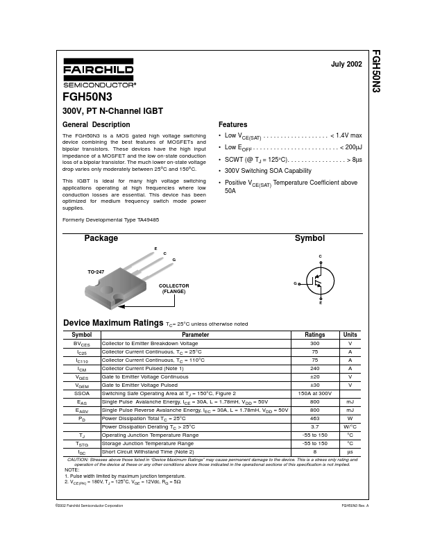
Package
Symbol
TO-247 COLLECTOR (FLANGE)
Device Maximum Ratings TC= 25°C unless otherwise noted
Symbol BVCES IC25 IC110 ICM VGES VGEM SSOA EAS EARV PD TJ TSTG t SC Parameter Collector to Emitter Breakdown Voltage Collector Current Continuous, TC = 25°C Collector Current Continuous, TC = 110°C Collector Current Pulsed (Note 1) Gate to Emitter Voltage Continuous Gate to Emitter Voltage Pulsed Switching Safe Operating Area at TJ = 150°C, Figure 2 Single Pulse Avalanche Energy, ICE = 30A, L = 1.78m H, VDD = 50V Single Pulse Reverse Avalanche Energy, IEC = 30A, L = 1.78m H, VDD = 50V Power Dissipation Total TC = 25°C Power Dissipation Derating TC > 25°C Operating Junction Temperature Range Storage Junction Temperature Range Short Circuit Withstand Time (Note 2) Ratings 300 75 75 240 ±20 ±30 150A at 300V 800 800 463 3.7 -55 to 150 -55 to 150 8 m J m J W W/°C °C °C µs Units V A A A V V
CAUTION: Stresses above those listed in “Device Maximum Ratings” may cause permanent damage to the device. This is a stress only rating and operation of...