MRF5S9080NBR1
MRF5S9080NBR1 is GSM/GSM EDGE LATERAL N-CHANNEL RF POWER MOSFETs manufactured by Freescale Semiconductor.
- Part of the MRF5S9080NR1 comparator family.
- Part of the MRF5S9080NR1 comparator family.
Features
- Characterized with Series Equivalent Large
- Signal Impedance Parameters
- Internally Matched for Ease of Use
- Qualified Up to a Maximum of 32 VDD Operation
- Integrated ESD Protection
- 200_C Capable Plastic Package
- Ro HS pliant
- In Tape and Reel. R1 Suffix = 500 Units per 44 mm, 13 inch Reel. Table 1. Maximum Ratings
Rating Drain- Source Voltage Gate- Source Voltage Storage Temperature Range Operating Junction Temperature Symbol VDSS VGS Tstg TJ
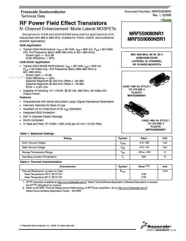
MRF5S9080NR1 MRF5S9080NBR1
- 960 MHz, 80 W, 26 V GSM/GSM EDGE LATERAL N
- CHANNEL RF POWER MOSFETs
CASE 1486
- 03, STYLE 1 TO
- 270 WB
- 4 PLASTIC MRF5S9080NR1
CASE 1484
- 04, STYLE 1 TO
- 272 WB
- 4 PLASTIC MRF5S9080NBR1 Value
- 0.5, +65
- 0.5, +15
- 65 to +150 200 Unit Vdc Vdc °C °C
Table 2. Thermal Characteristics
Characteristic Thermal Resistance, Junction to Case Case Temperature 79°C, 80 W CW Case Temperature 80°C, 36 W CW Symbol RθJC Value (1,2) 0.50 0.54 Unit °C/W
1. MTTF calculator available at http://.freescale./rf. Select Tools/Software/Application Software/Calculators to access the MTTF calculators by product. 2. Refer to AN1955, Thermal Measurement Methodology of RF Power Amplifiers. Go to http://.freescale./rf. Select Documentation/Application Notes
- AN1955.
© Freescale Semiconductor, Inc., 2006. All rights reserved.
MRF5S9080NR1 MRF5S9080NBR1 1
RF Device Data Freescale Semiconductor
Table 3. ESD Protection Characteristics
Test Methodology Human Body Model (per JESD22
- A114) Machine Model (per EIA/JESD22
- A115) Charge Device Model (per JESD22
- C101) Class 1B (Minimum) A (Minimum) IV (Minimum)
Table 4. Moisture Sensitivity Level
Test Methodology Per JESD 22
- A113, IPC/JEDEC...