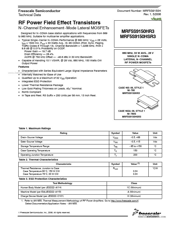
MRF5S9150HR3
MRF5S9150HR3 is SINGLE N-CDMA LATERAL N-CHANNEL RF POWER MOSFETs manufactured by Freescale Semiconductor.
Features
- Characterized with Series Equivalent Large
- Signal Impedance Parameters ..
- Internally Matched for Ease of Use
- Qualified Up to a Maximum of 32 VDD Operation
- Integrated ESD Protection
- Lower Thermal Resistance Package
- Low Gold Plating Thickness on Leads, 40μ″ Nominal.
- Ro HS pliant
- In Tape and Reel. R3 Suffix = 250 Units per 56 mm, 13 inch Reel.
MRF5S9150HR3 MRF5S9150HSR3
880 MHz, 33 W AVG., 28 V SINGLE N
- CDMA LATERAL N
- CHANNEL RF POWER MOSFETs
CASE 465
- 06, STYLE 1 NI
- 780 MRF5S9150HR3
CASE 465A
- 06, STYLE 1 NI
- 780S MRF5S9150HSR3
Table 1. Maximum Ratings
Rating Drain- Source Voltage Gate- Source Voltage Storage Temperature Range Case Operating Temperature Operating Junction Temperature Symbol VDSS VGS Tstg TC TJ Value
- 0.5, +68
- 0.5, +15
- 65 to +150 150 200 Unit Vdc Vdc °C °C °C
Table 2. Thermal Characteristics
Characteristic Thermal Resistance, Junction to Case Case Temperature 80°C, 150 W CW Case Temperature 76°C, 33 W CW Symbol RθJC Value (1) 0.34 0.34 Unit °C/W
Table 3. ESD Protection Characteristics
Test Methodology Human Body Model (per JESD22
- A114) Machine Model (per EIA/JESD22
- A115) Charge Device Model (per JESD22
- C101) Class 1C (Minimum) A (Minimum) III (Minimum)
1. Refer to AN1955, Thermal Measurement Methodology of RF Power Amplifiers. Go to http://.freescale./rf. Select Documentation/Application Notes
- AN1955.
© Freescale Semiconductor, Inc., 2006. All rights reserved.
MRF5S9150HR3 MRF5S9150HSR3 1
RF Device Data Freescale Semiconductor
Table 4. Electrical Characteristics (TC = 25°C unless otherwise noted)
Characteristic Off Characteristics Zero Gate Voltage Drain Leakage Current (VDS = 68 Vdc, VGS = 0 Vdc) Zero Gate Voltage Drain Leakage Current (VDS = 28 Vdc, VGS = 0 Vdc) Gate- Source Leakage Current (VGS = 5 Vdc, VDS = 0 Vdc) On Characteristics Gate Threshold Voltage (VDS = 10 Vdc, ID = 600 μAdc) Gate Quiescent Voltage (VDS = 28 Vdc, ID = 1500 m Adc, Measured in Functional Test) Drain- Source On
-...