The following content is an automatically extracted verbatim text
from the original manufacturer datasheet and is provided for reference purposes only.
View original datasheet text
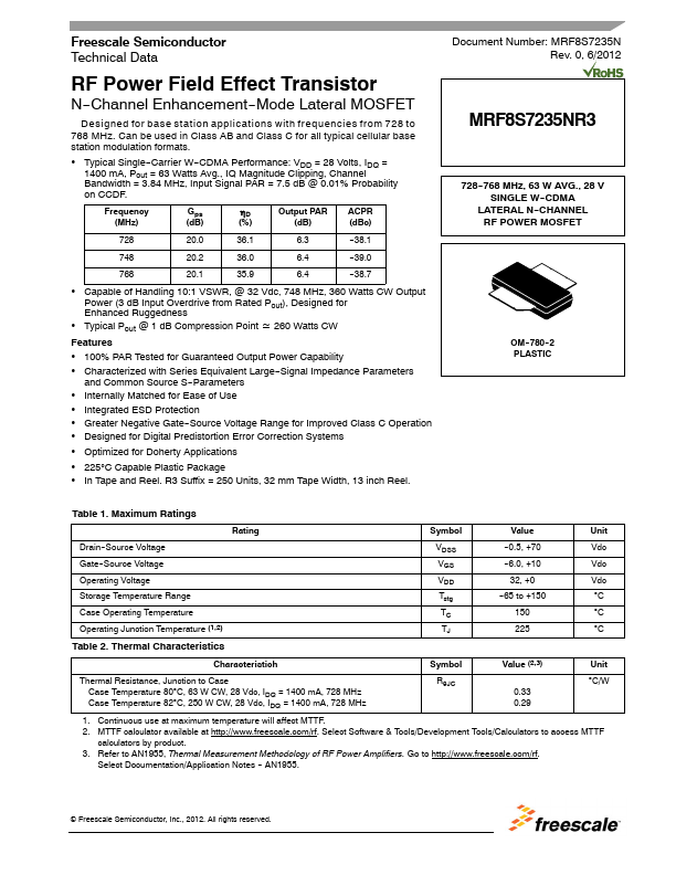
Freescale Semiconductor Technical Data
Document Number: MRF8S7235N Rev. 0, 6/2012
RF Power Field Effect Transistor
N--Channel Enhancement--Mode Lateral MOSFET
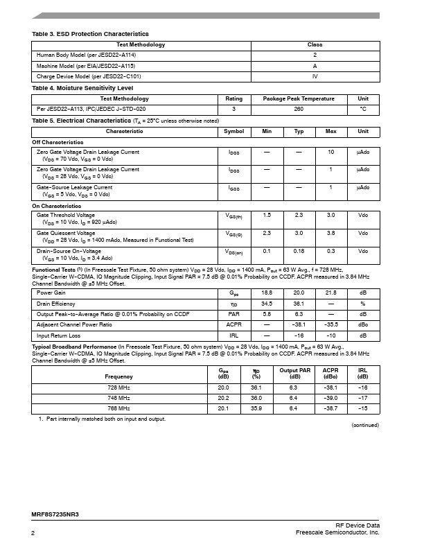
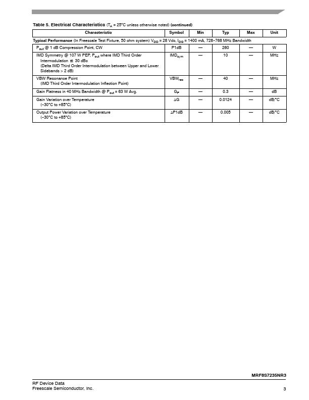
Designed for base station applications with frequencies from 728 to 768 MHz. Can be used in Class AB and Class C for all typical cellular base station modulation formats. • Typical Single--Carrier W--CDMA Performance: VDD = 28 Volts, IDQ = 1400 mA, Pout = 63 Watts Avg., IQ Magnitude Clipping, Channel Bandwidth = 3.84 MHz, Input Signal PAR = 7.5 dB @ 0.01% Probability on CCDF.
Frequency (MHz) 728 748 768 Gps (dB) 20.0 20.2 20.1 ηD (%) 36.1 36.0 35.9 Output PAR (dB) 6.3 6.4 6.4 ACPR (dBc) --38.1 --39.0 --38.7
MRF8S7235NR3
728-768 MHz, 63 W AVG.
 MRF8S7235NR3 Datasheet