MRFE6S9125NR1
MRFE6S9125NR1 is N-Channel Enhancement-Mode Lateral MOSFETs manufactured by Freescale Semiconductor.
- Part of the MRFE6S9125NBR1 comparator family.
- Part of the MRFE6S9125NBR1 comparator family.
Features
- Characterized with Series Equivalent Large
- Signal Impedance Parameters
- Internally Matched for Ease of Use
- Integrated ESD Protection
- 225°C Capable Plastic Package
- Ro HS pliant
- In Tape and Reel. R1 Suffix = 500 Units per 44 mm, 13 inch Reel. Table 1. Maximum Ratings
Rating Drain
- Source Voltage Gate
- Source Voltage Maximum Operation Voltage Storage Temperature Range Case Operating Temperature Operating Junction Temperature (1,2)
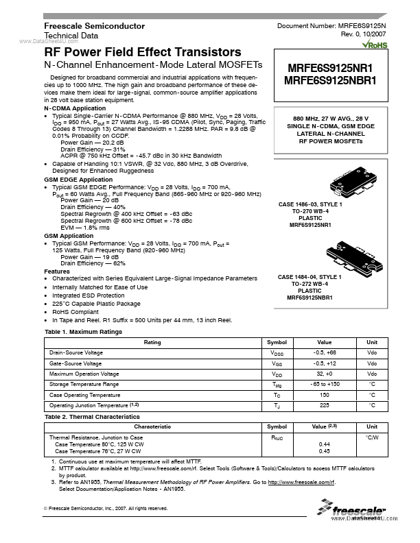
MRFE6S9125NR1 MRFE6S9125NBR1
880 MHz, 27 W AVG., 28 V SINGLE N
- CDMA, GSM EDGE LATERAL N
- CHANNEL RF POWER MOSFETs
CASE 1486
- 03, STYLE 1 TO
- 270 WB
- 4 PLASTIC MRF6S9125NR1
CASE 1484
- 04, STYLE 1 TO
- 272 WB
- 4 PLASTIC MRF6S9125NBR1
Symbol VDSS VGS VDD Tstg TC TJ
Value
- 0.5, +66
- 0.5, +12 32, +0
- 65 to +150 150 225
Unit Vdc Vdc Vdc °C °C °C
Table 2. Thermal Characteristics
Characteristic Thermal Resistance, Junction to Case Case Temperature 80°C, 125 W CW Case Temperature 76°C, 27 W CW Symbol RθJC Value (2,3) 0.44 0.45 Unit °C/W
1. Continuous use at maximum temperature will affect MTTF. 2. MTTF calculator available at http://.freescale./rf. Select Tools (Software & Tools)/Calculators to access MTTF calculators by product. 3. Refer to AN1955, Thermal Measurement Methodology of RF Power Amplifiers. Go to http://.freescale./rf. Select Documentation/Application Notes
- AN1955.
© Freescale Semiconductor, Inc., 2007. All rights reserved.
MRFE6S9125NR1 MRFE6S9125NBR1 1
RF Device Data Freescale Semiconductor
Table 3. ESD Protection Characteristics
.. Test Methodology Class 1B (Minimum) A...